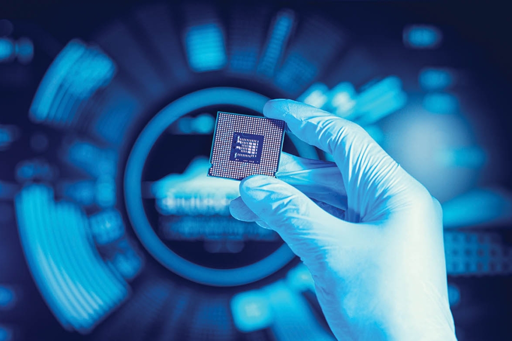
CEA-Leti and NcodiN partner to industrialise 300 mm Silicon Photonics
CEA-Leti and NcodiN, a French deep-tech startup pioneering
nanolaser-enabled photonic interconnects, have formed a strategic collaboration
to industrialize NcodiN’s optical interposer technology on a 300 mm integrated
photonics process.
NcodiN, which received €16 million in seed financing last
November, is developing optical interconnects designed to relieve a critical
data-movement bottleneck limiting performance in next-generation
semiconductors. The collaboration will accelerate the company’s
proof-of-concept work into industrial-grade 300 mm processes—moving beyond
copper interconnects and marking a major step toward scalable, in-package,
long-reach optical links for future computing architectures and artificial
intelligence (AI) chips.
As AI systems demand orders of magnitude increases in bandwidth and energy efficiency, the industry is shifting from copper to optical interconnects.
World’s smallest laser on silicon
NcodiN is building NConnect, the integrated optical
interconnect platform powered by the world’s smallest laser on silicon—500×
smaller than today’s industry-standard devices. The company’s nanolaser-enabled
photonic interposers pave the way to ultra-dense integration (>5,000
nanolasers/mm²) and record-low energy operation (~0.1 pJ/bit). Building on
CEA-Leti’s advanced photonics integration expertise, NcodiN is transitioning
its nanolaser to a 300 mm silicon photonics platform. This is a foundational
step toward scalable, wafer-level optical interconnects for high-end computing
and AI applications.

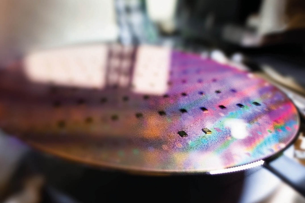
III-V semiconductor dies bonded to 300mm wafer using direct bonding and high-precision alignment. Credit : AUBERT/CEA
“NcodiN’s nanolaser-enabled photonic interconnects overcome the long-standing bottleneck of bulky, inefficient photonic components that have prevented large-scale adoption,” said Francesco Manegatti, co-founder and CEO of NcodiN. “Our collaboration with CEA-Leti aims to demonstrate NConnect’s compatibility with 300 mm wafers, which is essential for commercial-scale production and cost-effective adoption in AI-centric processors and high-bandwidth computing systems.”
‘Turning Point for Optical Interconnects’
Sébastien Dauvé, CEO of CEA-Leti, said the partnership
underscores the two parties’ shared commitment to enabling scalable photonic
infrastructure capable of meeting tomorrow’s computing demands.
“Transitioning photonics to a 300 mm CMOS-compatible process
is a turning point for optical interconnects that can finally be produced at
the scale, cost, and reliability the AI industry requires,” he said. “This
collaboration with NcodiN highlights a key part of CEA-Leti’s mission:
transferring advanced semiconductor and microelectronics technologies to
industry, where they serve a range of vital markets.”
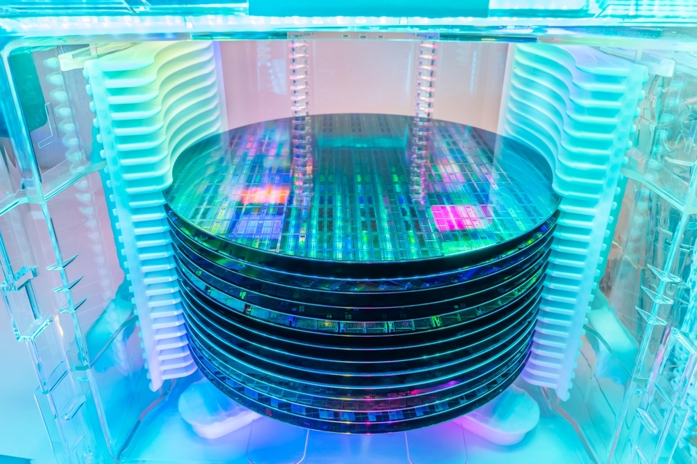
CEA-Leti and Fraunhofer IPMS validate wafer exchange
CEA-Leti and Fraunhofer IPMS have successfully completed the first exchange of ferroelectric memory wafers within the FAMES Pilot Line, marking a pivotal milestone in establishing a shared European platform for advanced embedded non-volatile memory (NVM) technologies. Launched in December 2023 and coordinated by CEA-Leti, the five-year initiative has demonstrated the viability of circulating complex material stacks across some of its leading research fabs.
The collaboration initially focused on the processing and electrical characterization of hafnium-zirconium oxide (HZO) ferroelectric capacitor stacks. Utilizing the combined 300 mm CMOS cleanroom capabilities of both institutes, they circulated the wafers in short process loops to enable joint evaluation of materials, electrode configurations, and device behavior.
The work also validated the wafer exchange and contamination-control protocols implemented in the pilot line, demonstrating that complex material stacks can be processed reliably across multiple advanced semiconductor facilities across all wafers.
The entire process adhered to standardized contamination control procedures, verified through VPD-ICP-MS (Vapor Phase Decomposition – Inductively Coupled Plasma Mass Spectrometry) and TXRF (Total Reflection X-Ray Fluorescence) analytics. Devices were evaluated using a ferroelectric capacitor (FeCAP) array test vehicle designed by CEA-Leti, with electrical characterization performed via the PUND (Positive-Up-Negative-Down) methodology to isolate true ferroelectric switching from parasitic effects.
Critical insights
“The successful wafer exchange marks an important step toward a joint European material-testing platform for ferroelectric memories,” said Dr. Wenke Weinreich, Division Director of Fraunhofer IPMS’ Center Nanoelectronic Technologies, a member of the 11-member FAMES consortium. “By combining our processing expertise with CEA-Leti’s CMOS integration capabilities, the pilot line provides a powerful environment for evaluating new ferroelectric stacks and accelerating their path toward system-level applications.”
Initial experimental results have already yielded critical insights. The team screened various electrode materials to enhance performance, finding that titanium nitride (TiN) bottom electrodes significantly outperform tungsten. In reliability tests, TiN exhibited lower failure rates after 10⁷ field cycles at 4 MV/cm. Furthermore, clear cross-split effects were observed across different electrode configurations, confirming the sensitivity of the test vehicles to process variations.
Seamless wafer exchanges across FAMES sites
“This first exchange between CEA-Leti and Fraunhofer IPMS
demonstrates that shared process flows, test vehicles, and characterization
environments can work seamlessly across FAMES sites,” noted Dominique Noguet,
pilot line coordinator and CEA-Leti vice president. “Establishing
reliable wafer loops between leading research fabs is essential for
accelerating ferroelectric memory development.”

Illustration of HfO₂-based ferroelectric devices enabling scalable, CMOS-compatible NVM. The architecture supports integration in both front-end (FeFET) and back-end memory structures, while opening pathways to advanced ferroelectric functionalities such as multiferroic, pyroelectric, and tunable RF devices. © Fraunhofer IPMS
Looking ahead, the wafer loops lay the groundwork for broader collaborative development. Upcoming phases will integrate HfO₂-based ferroelectric stacks from Fraunhofer IPMS into CEA-Leti CMOS processes, followed by array-level evaluations on GlobalFoundries’ 22nm FDX® Memory Advanced Demonstrator Multi-Project Wafer shuttle prepared by CEA-Leti. This builds on Fraunhofer IPMS’ recent completion of a first chip tape-out using the same 22nm FDX® technology, which also initiated research on algorithm-based AI compute-in-memory accelerator architectures.
The roadmap further includes studies on electrode process variations, long-term reliability, and back-end-of-line (BEOL) integration approaches, such as nanosecond laser annealing (NLA).
Together, these efforts advance the core mission of the FAMES Pilot Line: to provide a unified European platform for developing and validating emerging memory technologies—including OxRAM, MRAM, FeRAM, and FeFET.
By enabling collaborative material development and
standardized characterization, the initiative aims to strengthen Europe’s
capacity to design and manufacture the low-power, next-generation chip
architectures required for the future of computing.
CEA-Leti, CEA-List and PSMC
CEA-Leti and CEA-List, a specialist in smart digital systems, have announced a strategic collaboration with Powerchip Semiconductor Manufacturing Corporation (PSMC). The collaboration will leverage CEA-List’s RISC-V design expertise and CEA-Leti’s silicon photonics expertise to introduce high-bandwidth communication and high-efficiency computing technologies into PSMC’s established 3D stacking and interposer platforms to deliver solutions for next-generation artificial intelligence (AI) systems.
The semiconductor industry faces mounting challenges, including the physical limits of traditional copper interconnects, increasingly stringent power budgets, and the urgent need for flexible, scalable computing architectures. By integrating short-reach, high-bandwidth optical links for energy-efficient data movement and customizable RISC-V processor architectures, the collaboration directly addresses these constraints and establishes a new paradigm in high-performance data transport and computing architecture.
“RISC-V is transforming processor design by combining openness, flexibility, and cost efficiency. Its customizable architecture allows industrial players to develop solutions tailored to their needs,” said Olivier Thomas, Deputy Head of the Digital IC Design Division at CEA-List. “Our joint effort will give customers a customizable compute platform that meets the performance and power targets.”
“In the collaboration, microLED is a critical enabling technology that will boost optical-communication throughput using low-power GaN LED solutions,” added Sébastien Dauvé, Chief Executive Officer of CEA-Leti.
“This collaboration enriches PSMC’s 3D stacking and
interposer technology envelope with high-efficiency RISC-V computing IP and
high-bandwidth silicon photonics chiplet communication. By leveraging the
expertise of CEA-Leti and CEA-List alongside PSMC’s technologies, we will
provide foundry services to customers for next-generation AI applications,”
said Dr. Shou-Zen Chang, Chief Technology Officer of PSMC.
FAMES announces 2026 Open-Access Call
The FAMES Pilot Line has launched its second Open-Access Call for European semiconductor stakeholders to join the groundbreaking EU initiative focused on new chip architectures to boost European tech sovereignty. An online launch event was held this afternoon to provide researchers, academia, and industry teams with a detailed overview of the technologies currently available and the application process for accessing the pilot line.
Building on the strong interest and early silicon results of the 2025 open-access call, the 2026 program adds four new process design kits (PDKs) and research advances in integrated radio frequency filters and switches and components for power-management integrated circuits (PMIC).
Design houses, fabless companies, foundries, integrated
device manufacturers, material & tool suppliers, universities and research
centers can submit User Requests by responding to the two-month-long
Open-Access Call, starting today, or by submitting a Spontaneous User
Request throughout the year. For more information on the Open-Access
mechanisms, participants can download the User Guidelines and Procedures
document from the FAMES website
(https://fames-pilot-line.eu/guidelines-for-open-access/). Open-Access Calls
will take place each spring through 2028, with an updated portfolio of
available FAMES technologies.
New Process Design Kits
This year’s open-access call PDKs:
- 15 GHz LiNbO3 Bulk Acoustic Wave Resonator (BAW-SMR) Filter PDK and 7-15 GHZ AlN/ScAlN BAW RF Filter PDK, making these state-of-the-art highly miniaturized RF components, having band pass filtering capabilities in the FR3 range, accessible to the chip ecosystem,
- Phase Change Material-based RF switch PDK, allowing users to design their own demonstrators and integrate them for the first time on high-resistivity 300 mm silicon wafers,
- FAMES’ magnetics on silicon MagIC technology R&D samples and subsequent PDK, enabling users to integrate micro-inductors directly on their power management systems-on-chip, closest to the SoC load, and
- The FD-SOI 10nm pathfinding PDK release 1 for testing the capabilitiesof this advanced low-power technological node.
“The 2026 Open-Access Call supports the European Union’s sovereign technological strengths with enriched technologies thanks to two years of successful R&D results,” said Susana Bonnetier, open-access chairperson. “The radio frequency components PDKs are especially noteworthy this year, because for the first time, participants will be able to access and test sovereign 7-15 GHz acoustic RF filter and PCM switch technologies of their own design.”
Bonnetier explained that users will also be able to test the impact on power-delivery efficiency of integrating micro-inductors directly on their power-management ICs and explore the performance advantages of the FD-SOI 10nm technology node with the Pathfinding PDK that is now ready for licensing and delivery.
Launched in December 2023 by the Chips Joint Undertaking (Chips JU) and coordinated by CEA-Leti, FAMES envisions a strategic leap in semiconductor innovation, while reinforcing Europe’s industrial leadership. The FAMES project has two main objectives:
- To offer
Europe a domestic semiconductor pilot line
for advanced technologies
providing:
- Two generations of FD- SOI (Fully
Depleted Silicon-on-Insulator)
technology at the10nm and
7nm nodes,
- Various non-volatile memory (NVM)
options in metallic interconnects
above transistors,
- Radiofrequency (RF) components (passives,
switches, and
radio frequency filters), and
- 3D technological stacking options (3D
sequential integration
and 3D heterogenous integration),
- Seven application-driven demonstrators for brain computing interface, radar, neuromorphic computing, cybersecurity and optical communication networks.
- To promote FAMES Pilot Line technologies and to give Europe the opportunity to follow the miniaturization evolution of electronics on a wide spectrum of semiconductor markets strengthening European leadership and opening new opportunities.
In addition to the pilot line coordinator, France-based CEA-Leti, the FAMES consortium includes imec (Belgium), Fraunhofer (Germany), Tyndall (Ireland), VTT (Finland), CEZAMAT WUT (Poland), UCLouvain (Belgium), Silicon Austria Labs (Austria), SiNANO Institute (France), Grenoble INP (France) and the University of Granada (Spain).
FeFET wafer. © Fraunhofer IPMS