+44 (0)24 7671 8970
More publications     •     Advertise with us     •     Contact us
 
Loading...
News Article

Yongjiang Laboratory orders Reactive Ion Beam Trimming equipment from scia Systems

News

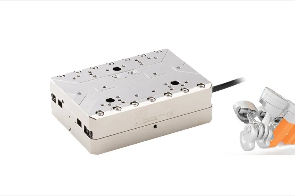
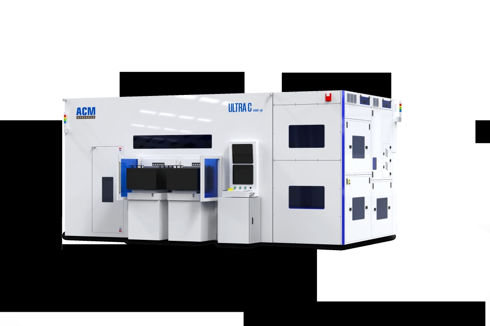
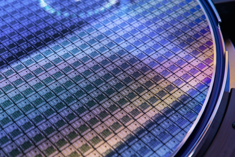
The scia Trim 200 system provides precise surface correction in film and wafer materials using ion beam trimming. The film thickness uniformity can be adjusted up to 0.1 nm.

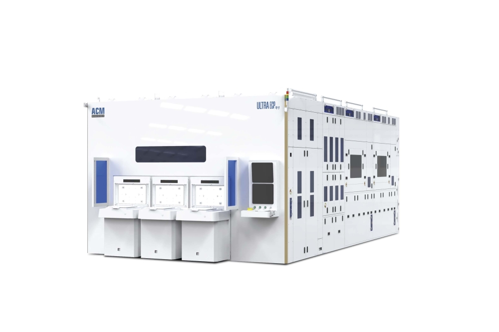
Yongjiang Laboratory (Y-LAB), a non-profit research and innovation center, established in 2021 in Zhejiang province, China, has purchased a scia Trim 200 system.

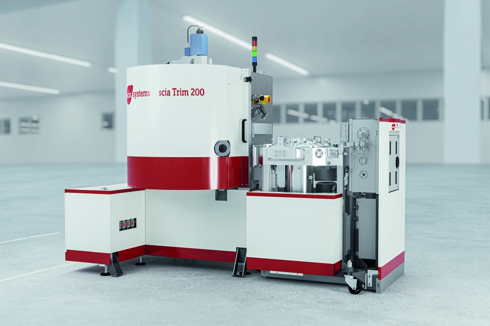
High-Precision Surface Correction with scia Trim 200

The scia Trim 200 guarantees high-precision film thickness trimming in wafer processing. Typical applications are frequency and thickness trimming in the manufacturing of acoustic-electrical devices and filters like bulk (BAW) or surface acoustic wave (SAW) filters, localized pole trimming of thin film head (TFH) applications, and dimensional correction of MEMS structures.

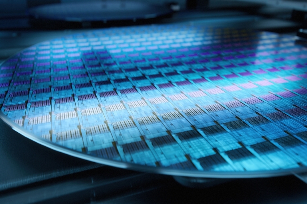
Designed for high-volume production and R&D applications, the system is equipped with a standard semiconductor cassette handling robot that accommodates wafers up to 200 mm in diameter.

The film trimming is performed by a focused broad ion beam with a sufficiently small focal point. The ion beam is directed to the substrate surface, causing a physical sputtering effect to remove material. During trimming, the wafer gets moved in front of the ion source by an x-/y-stage.

A metrology system detects the exact frequency topography map of each wafer area and converts this topography map into a coating thickness map. Based on that, the thickness of the coating that needs to be trimmed is calculated. Afterward, the internal control software of scia System calculates the corresponding dwell time map and follows the velocity scan profiles for the trimming process. By adjusting the local dwell time of the ion beam at specific positions, the system can control the local removal and etch non-uniformities, resulting in an impressive homogeneous film.

While ion beam trimming is done with noble gases like Argon, reactive gases can also be used for complex device structures to increase selectivity (reactive ion beam trimming, RIBT).

“We are proud that Y-Lab has opted for ion beam equipment provided by scia Systems for its laboratory. The scia Trim 200 offers a high degree of variability and is a good basis for future-oriented innovations and applied research thanks to its maximum flexibility in processing wafer materials without any restrictions and its ability to adjust the film thickness uniformity down to the atom level of 0.1 nm.” stated Dr. Michael Zeuner, CEO of scia Systems.

Advantest celebrates 25th anniversary of V93000 SoC Test Platform
Advanced packaging in Europe: Swissbit hosts EuroPAT Workshop 2024
Introducing the N-332 - Vacuum Compatible Nanopositioning Stage family
ACM Research strengthens its fan-out panel level packaging portfolio
Imec demonstrates logic and DRAM structures using High NA EUV Lithography
Yongjiang Laboratory orders Reactive Ion Beam Trimming equipment from scia Systems
Paving the way for the semiconductor future
Government scheme helps UK chip start-ups raise £10 million
Renesas completes acquisition of Altium
Greene Tweed highlights Chemraz 541
Intel acts to 'accelerate progress'
Infineon reports slight increase in revenue and earnings in Q3 FY 2024
New partnership brings semiconductor manufacturing to Central Valley
Merck joins German research project "Semiconductor-X"
V-Nova and Amlogic form partnership
AMI joins NXP Semiconductors Partner Program
EFC Gases & Advanced Materials announces $210 million investment
Promex Industries and QP Technologies implement sales/marketing reorganisation
Amkor signs preliminary Memorandum of Terms with US Department of Commerce
Ansys 2024 R2 delivers multiphysics innovation
Infineon introduces Edge AI evaluation kit
Nearfield Instruments to supply QUADRA Metrology System to Asian fab
ACM Research enters Fan-out Panel Level Packaging market
Nanotronics unveils nSpec ES
Samsung Electro-Mechanics collaborates with AMD
3D-Micromac receives laser-trimming system order from Infineon
Agile Analog delivers customisable IP on GlobalFoundries’ FinFet and FDX processes
Development of a fully digitised biological world
SkyWater invests in MEBL
Adeia enters into hybrid bonding agreement with Hamamatsu Photonics
Biden-Harris Administration unveils preliminary terms with GlobalWafers
UK-India Technology Security Initiative launches in New Delhi
×
Search the news archive

To close this popup you can press escape or click the close icon.
Logo
×
  • 1st January 1970
  • 1st January 1970
  • 1st January 1970
  • 1st January 1970
  • 1st January 1970
  • 1st January 1970
  • 1st January 1970
  • 1st January 1970
  • View all news 22645 more articles
Logo
×
Register - Step 1

You may choose to subscribe to the Silicon Semiconductor Magazine, the Silicon Semiconductor Newsletter, or both. You may also request additional information if required, before submitting your application.


Please subscribe me to:


You chose the industry type of "Other"

Please enter the industry that you work in: