Amkor signs preliminary Memorandum of Terms with US Department of Commerce

Amkor Technology has signed a non-binding preliminary memorandum of terms with the US Department of Commerce to receive proposed funding as part of the CHIPS and Science Act.
“This investment underscores the importance of advanced packaging in the semiconductor industry and reinforces Peoria’s position at the forefront of tech and innovation. This additional funding will further enhance local communities through quality job creation, while driving economic development growth for years to come.
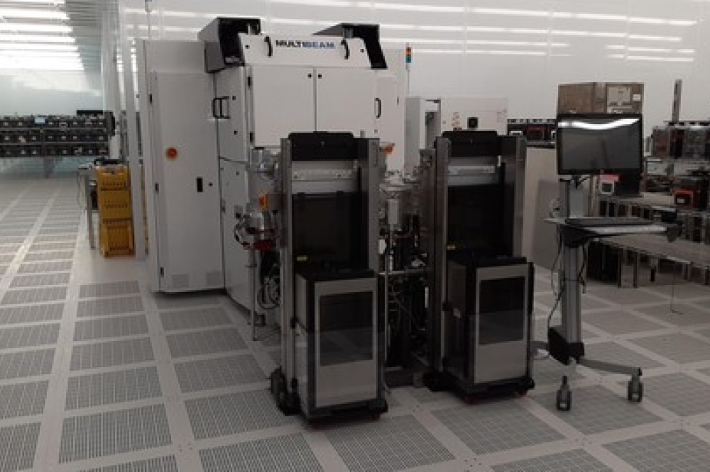
Amkor announced in November 2023 its plans to build its first domestic OSAT (outsourced semiconductor assembly and test) facility in Peoria, Arizona. Amkor projects to invest approximately $2 billion and employ approximately 2,000 people at the new facility. Upon completion, this will be the largest outsourced advanced packaging and test facility in the United States.
The terms include:
▶ Up to $400 million in proposed direct funding
▶ Access to $200 million in proposed loans
Amkor plans to take advantage of the Department of the Treasury’s Investment Tax Credit, which is expected to be up to 25% of qualified capital expenditures.
Amkor’s Arizona facility is an essential part to establishing a robust and resilient domestic semiconductor supply chain. Establishing an advanced packaging and test facility in Arizona allows Amkor to leverage its status as a strategic manufacturing partner for the world's leading semiconductor companies, foundries, and OEMs, while playing a significant role in ensuring competitive semiconductor manufacturing innovation in the US.
Commerce Secretary Gina M. Raimondo identified advanced packaging as a major area of focus for the US government’s effort to rebuild American semiconductor manufacturing. The Commerce Department emphasized that developing robust advanced packaging manufacturing capacity and capability is a key priority and essential to the success of the CHIPS program.
Amkor has secured approximately 55 acres with intent to build a state-of-the-art manufacturing campus with more than 500,000 square feet of clean room space. The first phase of the manufacturing facility is targeted to be ready for production within three years.
Amkor and TSMC have been working closely to provide high volume, leading-edge technologies for advanced packaging and testing of semiconductors to support critical markets such as high-performance computing, automotive, and communications. The companies’ shared vision is to enable seamless technology alignment for customers across a global manufacturing network.
Amkor first established its presence in the Greater Phoenix area in 1984 and is excited to expand its footprint in the evolving Arizona semiconductor industry. The new manufacturing location will uniquely position Amkor among a strong ecosystem of front-end fabs, IDMs, and suppliers with current or expanding presence in the area.
The project has garnered strong support as it expands the evolving semiconductor ecosystem, provides high-tech jobs, and increases economic energy in the Greater Phoenix area.
“Amkor is proud to be the leading advanced packaging and test OSAT headquartered in the US, and today’s announcement underscores our commitment to grow America’s domestic semiconductor ecosystem,” said Giel Rutten, Amkor’s president and chief executive officer. “Amkor’s Arizona facility will enable us to support the growing semiconductor manufacturing community—while creating 2,000 good jobs—and we look forward to providing our customers with domestic advanced packaging and test capabilities. Advanced packaging is an essential component of semiconductor innovation and manufacturing, and we appreciate our partners at the Department of Commerce for recognizing the importance of this sector as they work to support our industry.”
“One of the fundamental goals of the CHIPS and Science Act is creating an advanced packaging ecosystem in the U.S. to ensure full start to finish chip production occurs domestically. Advanced packaging drives chip innovation at all levels, and because of President Biden’s leadership, the U.S. will have a robust domestic footprint in this critical technology,” said U.S. Secretary of Commerce Gina Raimondo. “The leading-edge chips that will be packaged right here in Arizona are foundational to technologies of the future that will define global economic and national security for decades to come. Thanks to the Biden-Harris Administration, and Amkor’s investments in the U.S., this proposed funding would enhance our supply chain security, create thousands of jobs in Arizona, and further position the United States to out-innovate, out-build, and out-compete the rest of the world.”
“This announcement marks another significant milestone for President Biden and Vice President Harris’s CHIPS & Science Act – dramatically expanding advanced packaging capabilities in the United States,” said National Economic Advisor Lael Brainard. “Developing a comprehensive semiconductor ecosystem here in America, from R&D through packaging, will strengthen our technological leadership and create thousands of good paying jobs.”
“This is a big day for the state of Arizona and the entire country. With this award and Amkor’s significant investment, their new facility in Peoria will be one of the first advanced packaging facilities in the United States, marking a critical step in strengthening our microchip supply chain,” said Arizona Senator and chief negotiator of the CHIPS and Science Act Mark Kelly. “This project will create great-paying jobs, many of which won’t require a four-year degree. The CHIPS and Science Act is working for Arizona, providing new opportunities for our local workforce, and is working for our country, bringing back advanced manufacturing capabilities, and strengthening our national security.”