Loading...
News Article

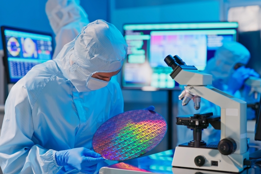
Tower Semiconductor releases 300mm silicon photonics process

News

Featuring 'industry-leading' figures of merit addressing the evolving needs for next-generation datacom applications.

Tower Semiconductor has released its new 300mm Silicon Photonics (SiPho) process as a standard foundry offering. This advanced process complements Tower's well-established 200mm (PH18) platform that is in high-volume production today, providing its customers with a cutting-edge solution tailored to meet the growing needs of high-speed data communications for next generation datacom applications.

The unique 300mm offering features best-in-class silicon waveguides and the most advanced low-loss silicon nitride waveguide offerings in the industry. The larger wafer size enhances compatibility with industry-standard OSAT (Outsourced Semiconductor Assembly and Test) platforms, facilitating seamless integration with electronic components and improving overall efficiency.

"We are proud to introduce our new, highly advanced Silicon Photonics offering, which provides a seamless path for our existing customers to transition to next-generation technology on 300mm wafers,” said Dr. Edward Preisler, Vice President and General Manager of RF Business Unit. “This process builds on Tower’s industry-leading 200mm SiPho platform both in terms of continuous process enhancements and increasing flexibility of supply for our customers."

Silicon photonics: accelerating growth in the race for high-speed optical interconnects
CCD-in-CMOS technology enables ultra-fast burst mode imaging
2025 6G A look forward
Critical Manufacturing climbs Deloitte’s Technology Fast 50
Semiconductors: The most important thing you probably know the least about
Imec and partners unveil SWIR sensor with lead-free quantum dot photodiodes
Lattice introduces small and mid-range FPGA offerings
SEMI and SMT inspection solutions at NEPCON Japan 2025
Nordic Semiconductor and Kigen demonstrate Remote SIM Provisioning for Massive IoT
Spirent collaborates with Siemens
Quobly forges strategic collaboration with STMicroelectronics
New standards in pressure measurement systems for the semiconductor industry
IBM delivers optics breakthrough
Semiconductor equipment sales to reach $139 Billion in 2026
Marvell introduces 1.6 Tbps LPO Chipset
ACM research strengthens Atomic Layer Deposition portfolio
CEA-Leti demonstrates embedded FeRAM platform compatible with 22nm FD-SOI node
Lattice introduces small and mid-range FPGA offerings
Solace unlocks full potential of event-driven integration
Advantest to showcase latest test solutions at SEMICON Japan 2024
CEA-Leti device integrates light sensing and modulation
Nordic launches Thingy:91 X prototyping platform for cellular IoT and Wi-Fi locationing
Imec achieves seamless InP Chiplet integration on 300mm RF Silicon Interposer
High-precision SMU
Powering India’s energy future
China’s Nvidia probe puts global investors ‘on notice’
POET Technologies appoints new director
Imec demonstrates core building blocks of a scalable, CMOS-fab compatible superconducting digital technology
Imec proposes double-row CFET for the A7 technology node
ULVAC launches new deposition system
Beebolt and SEMI Announce Strategic Partnership to Drive Supplier Resilience and Agility
esmo group introduces Automated Final Test Manipulator
×
Search the news archive

To close this popup you can press escape or click the close icon.
Logo
x
Logo
×
Register - Step 1

You may choose to subscribe to the Silicon Semiconductor Magazine, the Silicon Semiconductor Newsletter, or both. You may also request additional information if required, before submitting your application.


Please subscribe me to:


You chose the industry type of "Other"

Please enter the industry that you work in: