ams OSRAM receives EU Commission approval for investment grant

Investments in new generations of innovative microchips, which have now begun, totaling EUR 567 million by the time full production is reached in 2030, to meet increasing demand in applications such as automobile or medical technology, industry and consumer handhelds.
The European Commission has approved funding for a semiconductor manufacturing facility for ams OSRAM AG under the European Chips Act. The official funding approval from the Austrian Ministry of Economy and Labor, which is responsible for the payment of the funding, is now expected shortly. ams OSRAM plans to use the funding of up to €227 million approved by the European Commission to sustainably strengthen the development and production site in Premstaetten. In total, the company plans to invest 567 million euros in the project by 2030, when full production will begin at the headquarters in Styria.
“We are pleased that the European Commission has approved Austrian state aid under the European Chips Act to expand our semiconductor manufacturing in Premstaetten,” said Aldo Kamper, CEO of ams-OSRAM AG. ”The financing is part of ams OSRAM's important investments in Austria in new generations of innovative microchips for medical and automotive applications. The first fab of its kind for next-generation optoelectronic sensors is a key cornerstone of our growth strategy. In line with the objectives set out in the European Chips Act, it will strengthen Europe's security of supply and technological autonomy in the field of semiconductor technologies. We are grateful for the support we have received from both the Austrian government and the European Commission.”
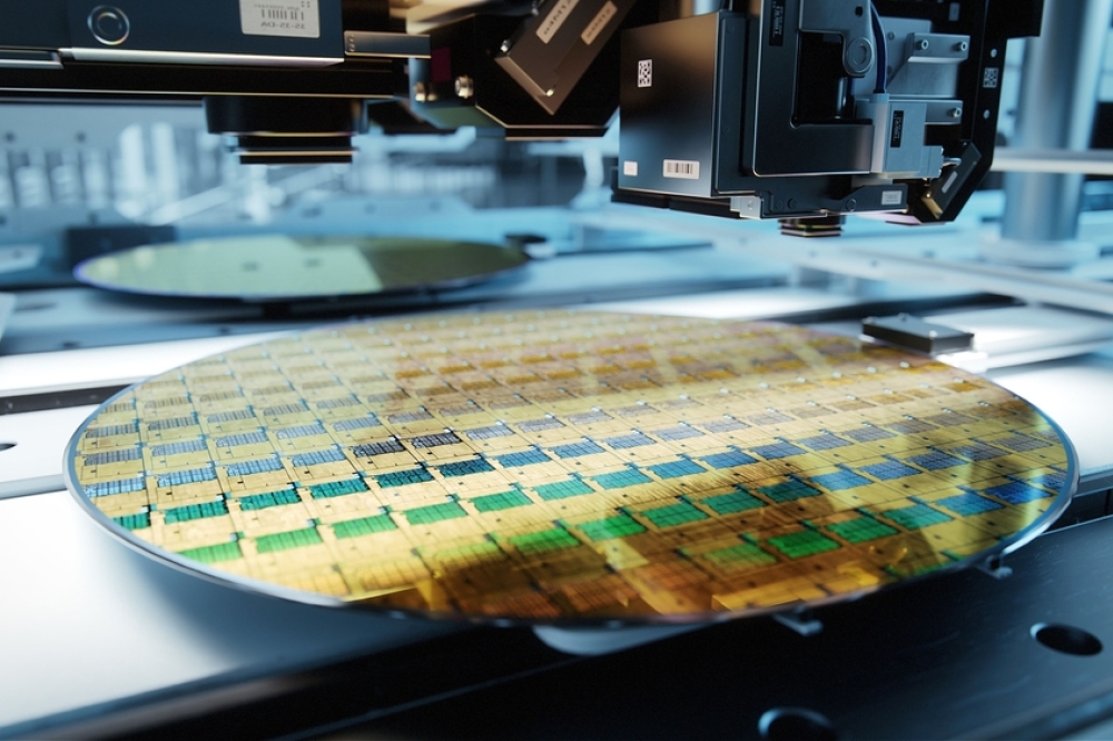
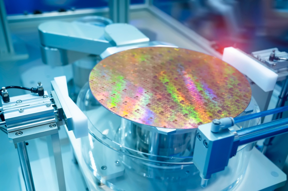
The new plant at the production site in Premstaetten is intended to further expand the leading role of the Austrian semiconductor industry. In the future, the semiconductor manufacturing facility will produce highly differentiated next-generation optoelectronic sensors that are qualified for applications in medical technology and the automotive industry. In addition, the production of products for industry or for use in consumer goods is planned. It combines outstanding technologies (CMOS, filter¹ and TSV²) and works according to a toolbox concept. Depending on the product, the different capabilities can be combined individually as required for energy-efficient products for imaging and optoelectronics with a reduced form factor, more functions on a single component and outstanding electrical performance. The construction of the additional cleanroom at the Premstaetten site, with an area of 1,800 square meters for CMOS production, will also double filter capacity and increase TSV capacity by a factor of four.
In view of the global situation in the semiconductor market, it is clear how important it is to invest in innovative key technologies for the future. That is why the European Commission has set itself the goal of promoting the mass production of semiconductors in Europe and increasing the global market share to 20 percent of production by 2030. In addition, new chip technologies for the next generation are to be made possible. The European Chips Act was created for this purpose. The investment of ams OSRAM will help to strengthen European sovereignty in semiconductor production and digitalization. It will also make an important contribution to the green transition.
1) Filters select incoming radiation. For example, they use the phenomenon of interference - the overlapping of light wavelengths - to pass or reflect certain spectral ranges of electromagnetic radiation. This enables color recognition beyond that of the human eye,
2) TSVs - Through Silicon Vias - are vertical electrical connections through a chip. They are essential building blocks for advanced packaging technologies for high performance, small footprint devices required in many different market segments such as consumer, automotive, medical, etc. Devices with TSVs are typically 30 to 70 percent smaller than conventional packaging concepts. Such a significant reduction in size is necessary to enable the implementation of sensors in Internet of Things applications.