Automated electronics disassembly
A new UN report finds that more and more electronic waste, or e-waste, is being produced worldwide—recycling efforts are not keeping pace, though.
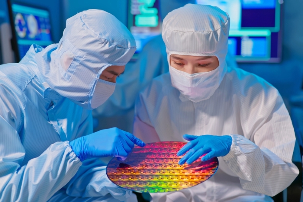
Valuable raw materials are not being recovered and recycled. Research scientists at the Fraunhofer Institute for Factory Operation and Automation IFF are tackling this issue. In the iDEAR project, they are developing solutions for automated, nondestructive robotic disassembly of electronics for remanufacturing and material recycling that will help establish an advanced circular economy.
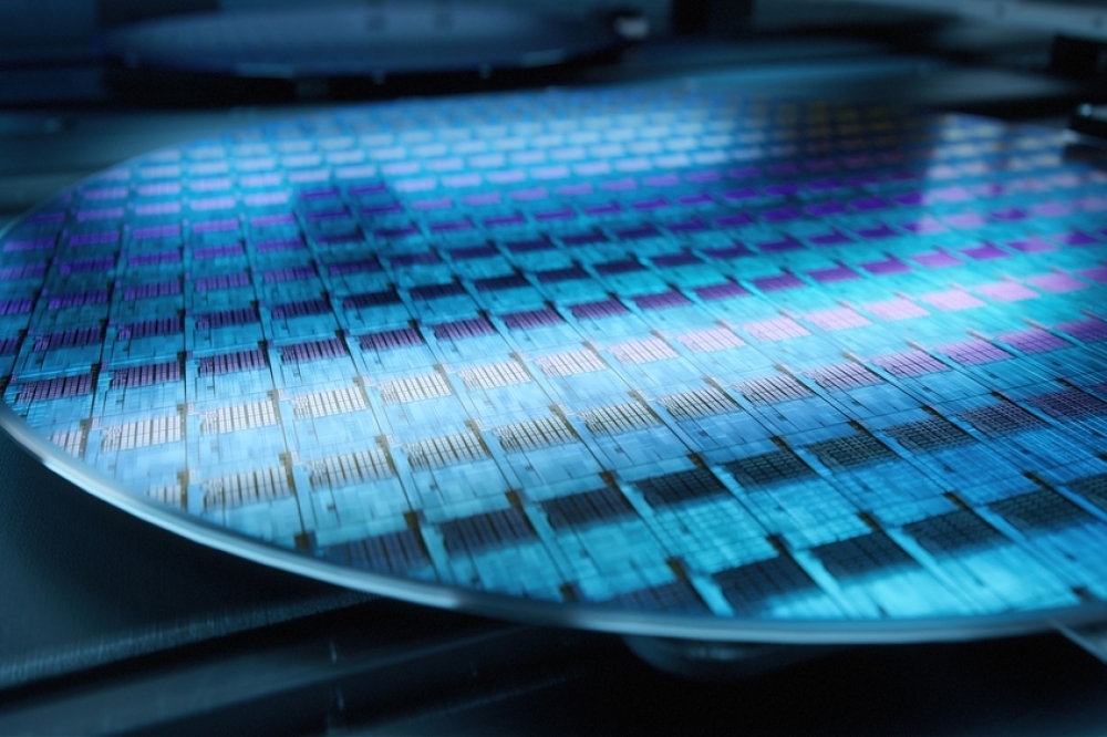
Advances in technology are steadily reducing the lifespans of electronic devices. This is resulting in steadily growing demand for finite raw materials. At the same time, e waste is continuing to pile up. Worldwide annual e-waste generation could rise to as much as 74 million metric tons by 2030. Only a small fraction of all electronic devices is recycled. Over 80 percent of the e-waste generated ends up in landfills or incinerators, including all the valuable raw materials, precious metals, and rare earths contained in the electronics. Incineration can release hazardous chemicals and substances into the environment.
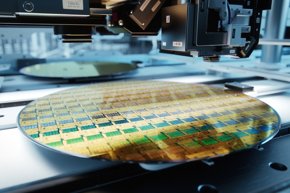
The small percentage of e-waste that undergoes treatment typically gets shredded, while only a limited portion is manually disassembled, cleaned of hazardous substances, broken down mechanically and sorted into different fractions. Such manual disassembly entails high costs and is not very effective, though. There have been virtually no sustainable value retention strategies to refurbish and recycle electronics that will enable an advanced circular economy. In the iDEAR project, short for Intelligent Disassembly of Electronics for Remanufacturing and Recycling, research scientists at Fraunhofer IFF in Magdeburg are combining knowledge management, metrology, robotics and artificial intelligence into an intelligent system for automated and nondestructive disassembly processes to establish a certifiable, closed-loop waste management system. “We intend to revolutionize the disassembly of e waste. Current solutions require substantial engineering and are limited to a particular product group. In the iDEAR project, we are pursuing a data-driven methodology so that as the widest variety of products, from computers to microwaves to home appliances, can be disassembled in real time with little engineering,” says Dr. José Saenz, manager of the Assistive, Service and Industrial Robots Group at Fraunhofer IFF. The research scientists are initially concentrating on the automated disassembly of computers. The system is intended to be upgradeable over time for any equipment, such as washing machines, for instance.
Automated identification of assemblies using high-precision metrology
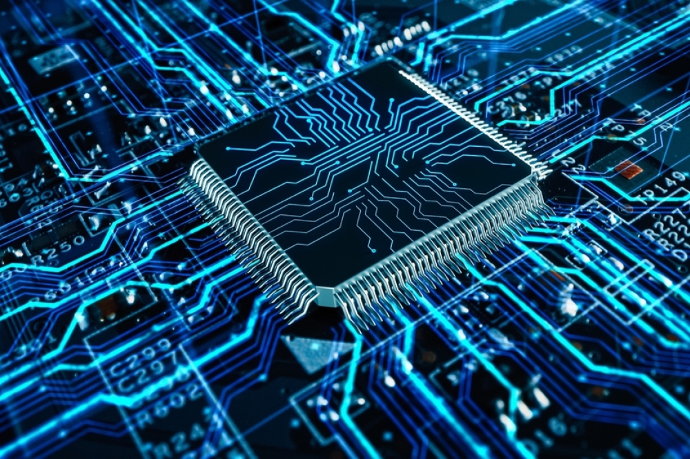
After the items have been delivered and separated, the initial processes of identification and condition analysis are initiated. Optical sensor systems and 3D cameras with AI-powered algorithms then scan labels with information on the manufacturer, product type and number, detect component types and locations, examine geometries and surfaces, assess the condition of fasteners, such as screws and rivets, and detect anomalies. “Optical metrology helps scan labels and sort different parts, such as screws, for instance. Previously trained machine learning algorithms and AI interpret the image data and enable the identification and classification of materials, plastics and components in real time based on sensor and spectral data,” Saenz explains. For instance, the AI detects whether a screw is concealed or rusted. All the data are stored in a digital disassembly twin, which is a product instance, so to speak, and also provides information on whether a similar product has ever been disassembled.
In the next step, Saenz and his team define the disassembly sequence so that their software can determine whether to execute a complete disassembly or only focus on the recovery of specific, valuable components. Glued or otherwise mated components hinder nondestructive disassembly. Rusty or stripped screws or deformed components are not ideal for this either. The disassembly process starts based on this high-level information. The robot receives a series of instructions and operations to complete, such as “Remove two screws on the left of the housing, open the housing” and so on. Whenever necessary, the machine changes each tool needed in between the individual steps. The skills specified in the disassembly sequences include robot actions, such as screwing, lifting, cutting, extracting, localizing, repositioning, releasing, moving levers, bending, breaking and cutting wires, which the disassembly robot can perform completely autonomously. The demonstrator even succeeded in tests to remove a motherboard from a computer—a very complex task that requires a high level of precision. “We used AI for that. An AI agent is initially trained to complete the process on the simulation model and later we transfer the trained robot action to the real-world experimental setup. This isn’t necessary for simple skills, such as localization. We use sensor and camera data for that,” Saenz explains.
The individual demonstrators for the subprocesses have been built: a station for the identification and analysis of computers, a demonstrator of the assessment model connected to the digital twin of the product and the disassembly sequence, a digital twin demonstrator, a demonstrator of the automatic execution of skills-based robot actions for disassembly and a demonstrator of AI generated robot actions to remove motherboards from the housing. In the next step, the demonstrators will be interconnected. The goal is one demonstrator that integrates all of the technological developments and can execute all of the of automated disassembly processes. “Recycling and remanufacturing are a key for manufacturing companies to ensure access to raw materials. The recovery of these materials not only reduces the environmental impact of e waste but also constitutes a valuable source of raw materials for new products,” Saenz says.