Thalia introduces latest version of AMALIA

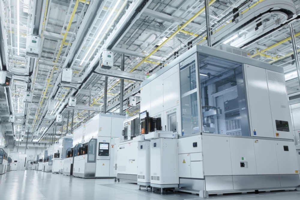
Thalia Design Automation has announced the immediate availability of the latest version of the AMALIA Suite, their AI-powered industry end-to-end IP reuse platform.
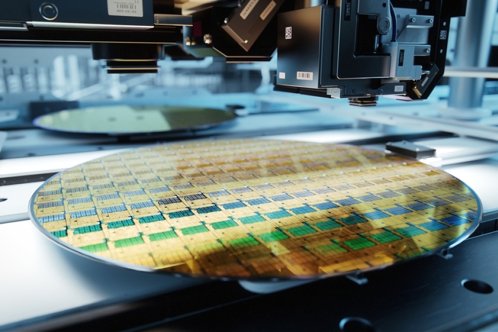
This release brings significant enhancements throughout AMALIA, particularly within its Layout Automation Suite. The solution retains the intrinsic value of production silicon, delivering the final step in the design migration flow. It employs a custom AI Design Transformer engine for analog physical implementation, leveraging the source layout and PDK. The migrated layout maintains the existing floorplan, ensuring DRC/LVS integrity. With AMALIA, customers can have a dedicated solution to the challenge of analog and mixed-signal migration and reliably achieve migration design time savings of up to 40%.
“Our mantra is to continually drive down migration design cycle time and we achieve this with dramatic steps at each major release of AMALIA,” said Thalia’s CEO, Sowmyan Rajagopalan. “We’ve introduced a game-changer within the Layout Automation Suite with a new device-stretching algorithm, metal stacking, along with significant functionality enhancements to automate the identification and migration to Flip Well designs for FDSOI.”
IP layout migration from one silicon process to another often encounters challenges due to varying PCell sizes. This results in open and shorts when trying to maintain the floor plan between the source and target technology. Fixing this manually can be a very time consuming. AMALIA’s new ‘device-stretching’ algorithm solves this issue while preserving the floorplan, delivering DRC-clean results, and promising substantial time savings.
For designs migrating to or from FDSOI, new analysis capabilities in AMALIA’s Technology Analyzer solution can identify standard transistor versus Flip Well devices and their unique electrical connection requirements, This knowledge seamlessly carries through to the Circuit Porting phase of migration, where AMALIA efficiently guides the user with their relevant design options.
These new capabilities – the device stretching algorithm, metal stacking and the analysis for Flip Well devices – represent significant advances in AMALIA.Thalia’s customers have experienced design cycle time reductions of up to 40%, thanks to continuous advances in the tool suite. This latest product release reinforces AMALIA’s unique position in analog design and IP migration.
Summary of capabilities added to AMALIA products in release 24.4
• Layout Automation Suite
• New device-stretching algorithm
• Smart vias porting to achieve DRC-clean vias
• Improved device mapping generator
• Devices shifting based on layer combination
• Design Enabler
• Enhancements to rapidly identify devices that impact circuit performance
• Circuit Porting Suite
• Flip well identification and related unique connections
• Conditional device mapping and improved generator
• Circuit area calculation
• Technology Analyzer
• Preference driven device mapping
• Flip Well design recognition in FDSOI process technology
• AI device recognition and analysis
• Enhanced waveform interpolation algorithm