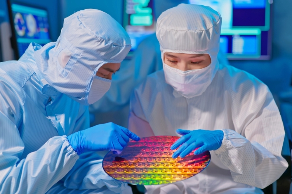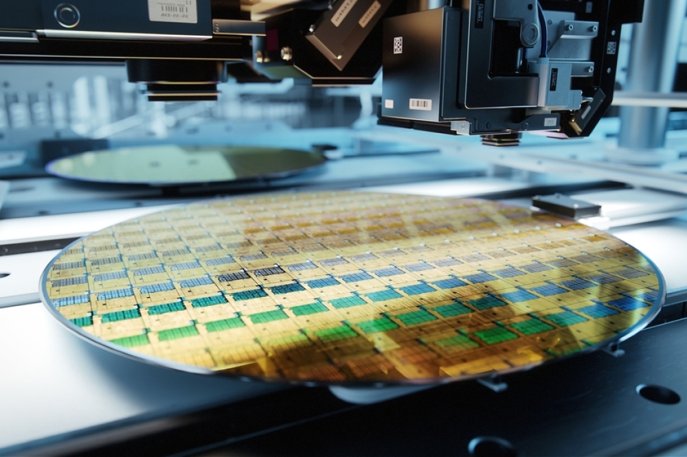
Current scenario of the semiconductor wafer industry

Recent developments that have impacted the market’s landscape.
By Koyel Gosh, Team Lead, Allied Market Research.
The increasing demand for electronic devices in consumer and industrial settings has led to substantial growth in the semiconductor wafer industry. The market’s landscape has changed significantly due to the introduction of new products, mergers, acquisitions, and other recent developments.
One noteworthy development in the industry is the growing demand for 5G technology. As the world moves toward a more connected future, 5G technology is expected to be the backbone of this network. As a result, demand for semiconductors used in 5G technology has grown exponentially. Companies such as TSMC (Taiwan Semiconductor Manufacturing Company) and Samsung have already started producing 5G chips on their 7nm process node.
Another recent development is the increased demand for electric vehicles (EVs). As the world moves toward cleaner energy solutions, EVs are becoming more and more popular. Semiconductors are necessary components to operate vehicles, especially in power electronics where Insulated Gate Bipolar Transistors (IGBTs) are commonly used. This growing demand has resulted in a shortage of semiconductors, particularly those used in the automotive sector.
Growing demand for digitization has propelled the industry in more than one way.
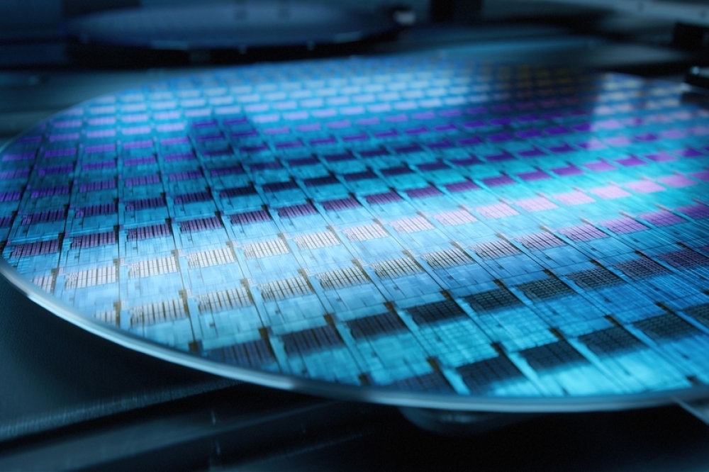
The semiconductor industry plays a crucial role in driving innovation across various sectors such as electronics, automobiles, and automation. The core component of many microelectronic devices, the semiconductor silicon wafer, has become increasingly important with the rising demand for digitization and electronic mobility. As gadgets become smaller, there is a need for more functionalities from a single device, which means that integrated circuit (IC) chips should have more transistors to support additional features.
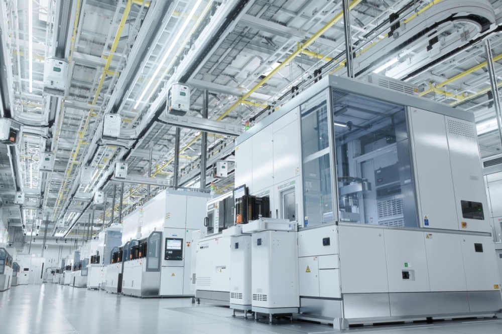
To keep up with these demands, foundries are investing in advanced packaging techniques, particularly those based on silicon wafers. Researchers are currently investigating the use of two-dimensional materials in the development of Monolithic 3D Integrated Circuits as a possible alternative to silicon, with the goal of improving transistor density. For example, TSMC has developed a technology called “chip on wafer on substrate,” which features the world’s largest silicon interposer, measuring nearly 2500mm2. This interposer can accommodate two 600mm2 processors and eight HBM memory devices in a 75mm2 package. These advancements and innovations in the semiconductor industry are significantly impacting downstream technologies. Keeping in tab with a recent report by Allied Market Research, the global semiconductor wafer market is anticipated to exhibit a considerable CAGR from 2021 to 2030.
Wearable devices are set to provide significant growth opportunities for the market vendors too, especially in the industrial sector, where they have the potential to improve quality and safety. Siemens predicts that the market for industrial wearables will be substantial. Zebra Technologies Corporation forecasts that 40-50% of global manufacturers will have adopted wearable technology by 2022. In addition, there has been a rise in the desire for compact electronic devices, leading to an expectation for increased capabilities and features within a single gadget. As a result, IC chips will need to incorporate more transistors to support these additional features.
Emerging economies such as China have implemented government policies that are favorable to the semiconductor industry. This has created significant growth opportunities in the semiconductor silicon wafer market, which is expected to continue expanding in the forecast period. One example of such policies is the framework issued by the State Council of the People’s Republic of China, which prioritizes the development of advanced semiconductor packaging solutions within the industry.
The Consumer Technology Association’s study on US consumer technology sales and forecast predicts that 5G-enabled smartphones will see significant growth in 2021, with 2.1 million units sold and over USD 1.9 billion in revenue. Meanwhile, Apple has announced plans to contribute USD 350 billion to the US economy by 2023 and create 2.4 million jobs over the next five years through new investments and spending with domestic companies. Apple’s recent announcement is expected to drive up the demand for semiconductor silicon wafers, given their significant presence in the consumer electronics industry.
Innovative product launches by companies
The Singapore-MIT Alliance for Research and Technology (SMART) has recently made an announcement regarding their successful development of a way to manufacture integrated silicon III-V chips that contain high-performance III-V devices. While silicon-based CMOS chips are widely used for computing purposes, they are not as efficient when it comes to communication and illumination. This results in lower efficiency and increased heat generation, causing 5G mobile devices to become hot and shut down quickly. In order to deal with the issue, it is essential to integrate III-V semiconductor devices with silicon. However, this has been a complex challenge for the semiconductor industry to overcome. SMART’s accomplishment represents a significant step towards solving this issue in a commercially viable manner.
The semiconductor wafer market is characterized by rapid innovation, and companies are continually launching new products to meet the demands of the market. One recent product launch worth mentioning is Intel’s 11th Gen Core Processors. The processors use Intel’s 10nm SuperFin technology, which allows for improved performance and power efficiency. The launch of these processors has caused a shift in the market, with other companies rushing to release similar products.
TSMC, a major semiconductor manufacturer, recently announced its plans to invest USD 12 billion between 2021 and 2029 towards constructing a 12-inch wafer plant that will produce chips using the advanced 5 nm process. This indicates a positive trend towards the growth of the semiconductor industry in North America. Additionally, the relocation of tech supply chains from foreign countries to North America is expected to continue, even after the change in political leadership from Donald Trump to Joe Biden, who had previously encouraged foreign companies to invest and create employment opportunities in the United States. Furthermore, the United States has some of the world’s major players in the automotive industry, who are investing in electric vehicles and the self-driving potential of cars. This is fueling the demand for high-performance Integrated Circuits (ICs) in the semiconductor silicon wafers market.
The notable mergers and acquisitions in the industry
Mergers and acquisitions have also become prevalent in the semiconductor wafer market, as companies aim to broaden their product range and enhance their technological capabilities. One notable example of such a merger is the acquisition of Arm Holdings by NVIDIA. Arm Holdings is a major provider of semiconductor intellectual property, and NVIDIA’s purchase of the company will enable it to extend its footprint in the data center and AI sectors.
Intel’s recent acquisition of GlobalFoundries, one of the leading semiconductor foundries, is worth noting indeed. By acquiring GlobalFoundries, Intel aims to bolster its manufacturing capabilities and better compete with key players in the industry such as Samsung and TSMC. The acquisition is expected to be completed by the end of 2021.
On the other hand, SK Siltron Co. has recently announced that it plans to invest 1.05 trillion in the next three years to expand its facilities for 300 mm wafers located in Gumi National Industrial Complex 3. GlobalWafers Co., a top-notch silicon wafer supplier in the world, is set to begin expansion work in 2022, with mass production slated to start in 2024. The company anticipates adding roughly 20,000 state-of-the-art 12-inch wafers per month from its local fabs as a result of this expansion. The company anticipates that this expansion will increase its capacity by 10-15% at its plants in South Korea, Japan, Taiwan, and Italy, thereby meeting the robust demand for its products.
Shin-Etsu Chemical Co. Ltd has recently declared a 10 percent increase in the pricing of all its silicone goods, and one of its business areas will be expanded in Japan and worldwide. As a result, there has been a significant surge in prices, along with increased transportation costs for raw materials procurement and finished goods distribution.
Experts at the Massachusetts Institute of Technology have developed a method for creating thin transistors directly on top of computer chips using automation technology-
MIT researchers have developed a new technology that can “grow” ultrathin 2D materials directly on top of a fully fabricated silicon chip, enabling the creation of denser and more powerful computer chips. This is a significant development as semiconductor chips traditionally use bulk materials that are difficult to stack to create denser integrations. The challenge has been that the process of growing 2D materials on a silicon wafer requires temperatures of about 600 degrees Celsius, which can damage the silicon transistors and circuits that cannot be heated above 400 degrees. The interdisciplinary team of MIT researchers has overcome this challenge by developing a low-temperature growth process that does not damage the chip. This process allows 2D semiconductor transistors to be directly integrated on top of standard silicon circuits. The latest technology has the capability to grow a consistent layer of TMD material on an entire 8-inch wafer in less than 60 minutes, which represents a substantial reduction in the time required to cultivate these materials uniformly. This new process of developing 2D materials directly onto a silicon wafer is a major advancement as it avoids imperfections that can occur when transferring the material from elsewhere and enables the creation of denser and more powerful computer chips.
The researchers focused on a 2D material called molybdenum disulfide, which has excellent electronic and photonic properties and is suitable for use in semiconductor transistors. This material is made up of a layer of molybdenum atoms sandwiched between two layers of sulfur atoms, and it is flexible and transparent.
To grow thin films of molybdenum disulfide, a process called metal-organic chemical vapor deposition (MOCVD) is often used. The process involves subjecting two organic compounds containing molybdenum and sulfur atoms to temperatures exceeding 550 degrees Celsius.
This leads to their decomposition into smaller molecules that subsequently combine to form chains of molybdenum disulfide on a surface. However, the use of such high temperatures poses a challenge, as it can cause the degradation of silicon circuits, which begin to break down above 400 degrees.
A new furnace has been devised for the MOCVD (metal-organic chemical vapor deposition) process, which consists of two chambers: one for placing the silicon wafer at a low temperature, and the other for heating the precursors to a high temperature (above 550 degrees Celsius). The molybdenum precursor is kept in the low-temperature region to prevent damage to the silicon wafer and is decomposed at a temperature below 400 degrees Celsius. Meanwhile, the sulfur precursor is allowed to flow into the high-temperature region, where it is decomposed, and then returns to the low-temperature region for the chemical reaction that facilitates the growth of molybdenum disulfide on the surface of the wafer.
The specialists also developed a new method for growing molybdenum disulfide on silicon wafers using metalorganic chemical vapor deposition (MOCVD). They found that placing the wafer vertically in the low-temperature area of the furnace allowed for better material uniformity, as the gas molecules swirled around the chip and improved the growth of the material. This method was also much faster than traditional MOCVD processes, with a layer being grown in less than an hour compared to a full day. The vertical placement of the wafer ensured that no part of it was damaged by the heat, as neither end was too close to the high-temperature region. The scientists have utilized the advanced MIT. Nano facilities to exhibit excellent quality and uniformity of materials over an 8-inch silicon wafer. This achievement holds significant importance for industrial applications that require larger wafers. The process used to achieve this outcome is highly efficient, as it reduces growth time and can be easily incorporated into industrial processes. Additionally, the process is compatible with low-temperature silicon, which makes it feasible to extend the use of 2D materials in the semiconductor industry.
The technologists aspire to improve their techniques and apply them towards the development of multiple layers of 2D transistors stacked on top of each other, with the goal of enhancing their functionality and performance. They also plan to explore the use of the low-temperature growth process for flexible surfaces such as polymers, textiles, or papers. The successful application of this process could enable the integration of semiconductors into everyday objects like clothing or notebooks.
The funding for this project has been provided by a diverse range of organizations including the National Science Foundation Center for Integrated Quantum Materials, Ericsson, the U.S. Department of Energy, the U.S. Army Research Office, MITRE, and the MIT Institute for Soldier Nanotechnologies. The project has also received support from TSMC University Shuttle.

Koyel Gosh, Team Lead, Allied Market Research.