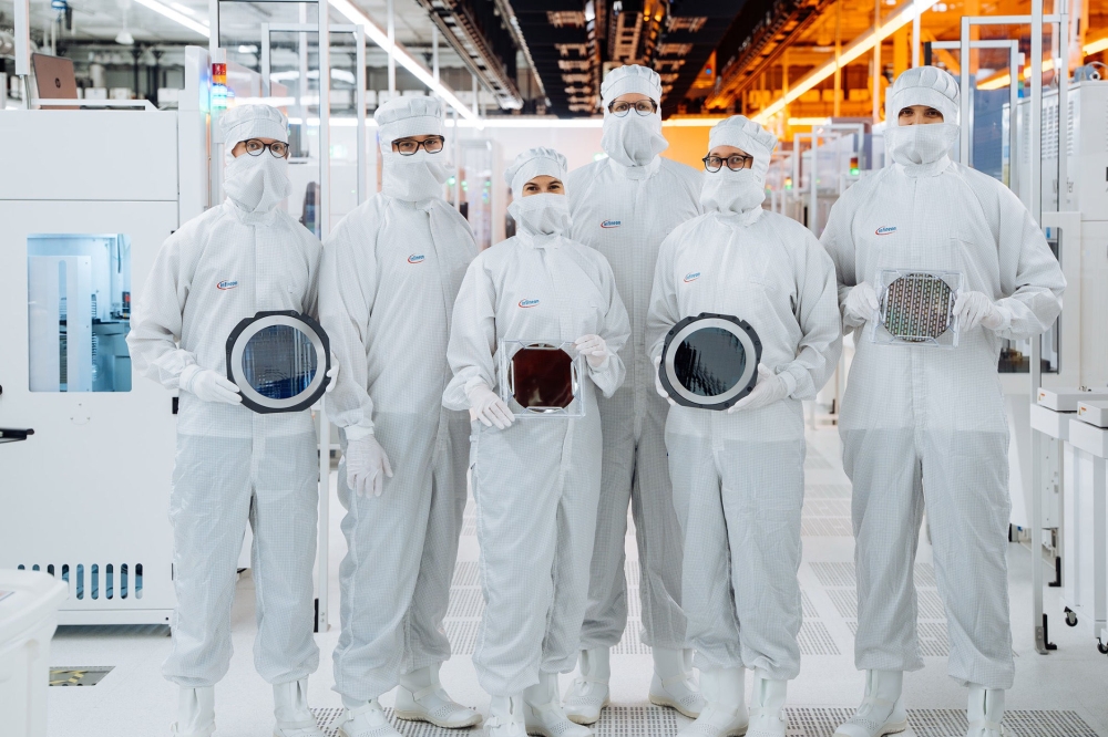
Imec unlocks lever for EUV dose reduction

Oxygen injection during metal-oxide resist post-exposure
bake emerges as game-changer for throughput.
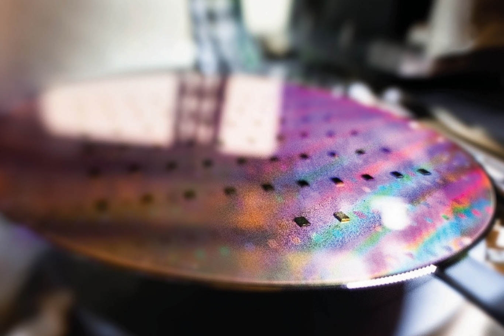
- At the 2026 SPIE Advanced Lithography + Patterning Conference, imec demonsrated that precise control of gas compositions during post-exposure EUV lithography steps can help in minimizing the required exposure dose, thereby unlocking higher wafer throughput. In particular, improved dose response of metal-oxide photoresists (MORs) has been achieved when the EUV post-exposure bake step is performed under elevated oxygen concentrations.
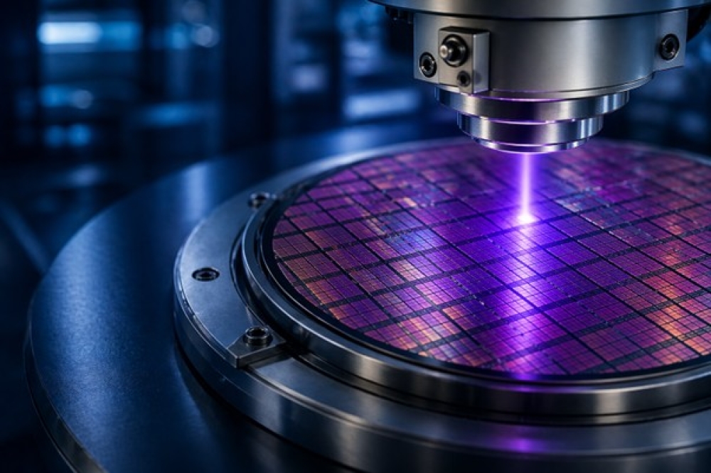
Metal-oxide resists (MORs) have emerged as leading
candidates for advanced EUV lithography applications, offering superior
resolution, reduced line-edge roughness, and good EUV dose-to-size performance
compared to chemically amplified resists (CARs). Their better pattern transfer
capability for small features and thin resist films makes them particularly
attractive for the highest resolution metal layers, exposed using High NA EUV
lithography. Imec now demonstrates that the dose response of MORs can be further
improved by raising the oxygen concentration above atmospheric levels during
the EUV lithography post-exposure bake step – a critical heat treatment step
after EUV resist exposure and before resist development.

Ivan Pollentier, Senior Researcher at imec: “We observe a 15-20% faster photo-speed when increasing the oxygen concentration from atmospheric 21% to 50% during post-exposure bake. The trend is observed for both model MOR and commercial MOR materials. This finding shows for the first time that carefully controlling the gas composition during key lithography steps can significantly cut the required EUV exposure dose, directly boosting the throughput of the EUV scanner and reducing process costs. This is just a first result from the BEFORCE tool: the controlled gas composition provides an additional knob to study the origins of environmental effects on the lithographic variability of MOR materials. Equipment manufacturers can use these insights as a guideline to adapt their tools for improved EUV lithography throughput and stability.”
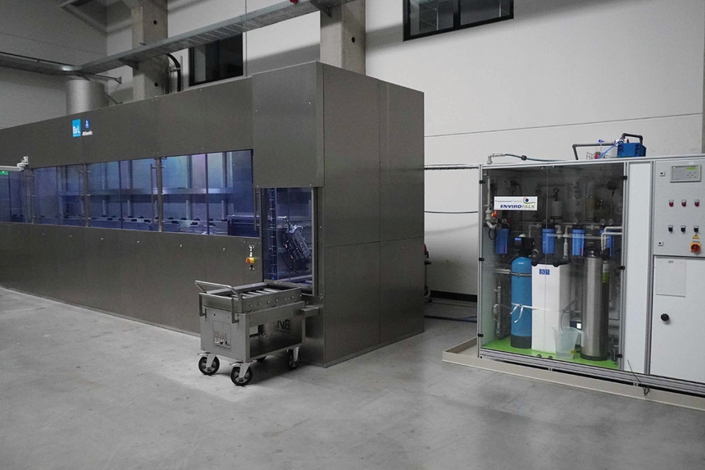
The results were achieved using BEFORCE, a unique research tool developed by imec to investigate the role of the ambient environment on critical dimension (CD) stability and performance of MORs. Kevin Dorney, R&D Team Lead at imec: “In commercial EUV clusters, resist-coated wafers are exposed in vacuum and then transferred to the post-exposure bake unit, where they are heated under atmospheric conditions. Our BEFORCE tool mimics these operations, but the wafer transfer and post-exposure bake are isolated from the cleanroom atmosphere and can be performed in precisely controlled environments allowed by gas injection and mixing systems. This unique ability, in combination with an integrated photo-speed measurement, was key to revealing the role of oxygen in boosting MOR’s dose response.”
To optimally exploit the positive impact of gas compositions
on the MOR performance, a more fundamental understanding of the chemical
mechanism at play during the resist’s post-exposure bake is essential.
Experiments are ongoing to correlate MOR performance to observations of
chemical changes during bake – captured by an integrated Fourier transform
infrared spectrometer – under varying environmental conditions. The planned
expansion of the BEFORCE tool with advanced metrology capabilities will enable
imec to drive even more impactful results.
BEFORCE can be used more broadly to study both MOR and CAR resists and is accessible to imec’s partners for resist evaluation.
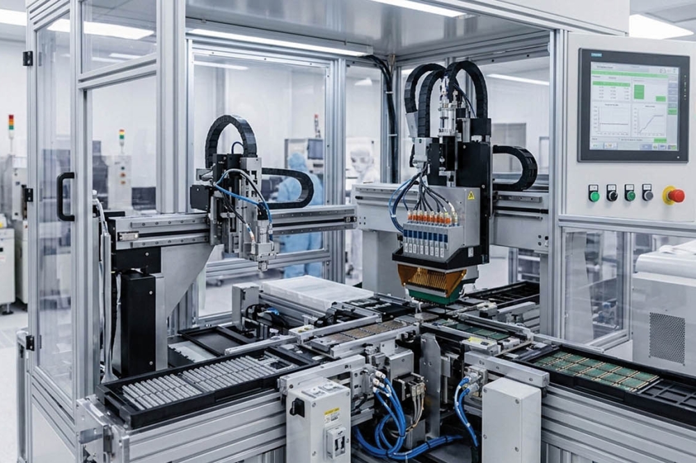
The world’s most advanced High NA EUV system
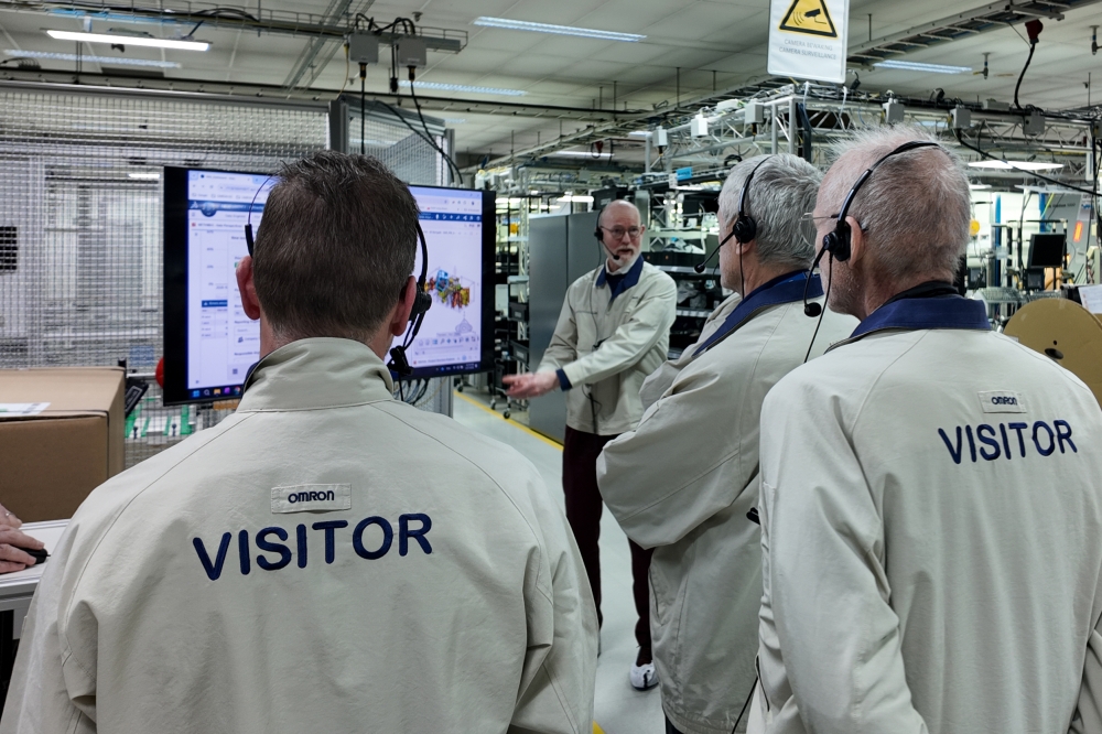
Recently, imec received delivery of the ASML EXE:5200 High NA EUV lithography system, the most advanced lithography tool available today. With this strategic milestone, imec reinforces its position as the industry’s launchpad into the ångström era, giving its global partners ecosystem unparalleled early access to the next generation of chip-scaling technologies. Integrated directly with a comprehensive suite of patterning and metrology tools and materials, the High NA EUV system will empower imec and its ecosystem partners to unlock the performance needed to pioneer sub-2nm logic and high-density memory technologies that will fuel the rapid growth of advanced AI and high-performance computing.
Luc Van den hove, CEO of imec: “The past two years have marked an important chapter for High NA (0.55NA) EUV lithography, with imec and ASML joining forces with the ecosystem in its joint High NA EUV Lithography Lab in Veldhoven (The Netherlands) to pioneer High NA EUV technology. With the installation of the EXE:5200 High NA EUV lithography system into our 300mm cleanroom in Leuven (Belgium), we aim to bring these High NA EUV patterning technologies to an industry-relevant scale and to develop the next-generation High NA EUV patterning use cases. Its unmatched resolution, improved overlay performance, high throughput, and a new wafer stocker that improves process stability and throughput, will give our partners a decisive advantage in accelerating the development of sub-2nm chip technologies. As the industry moves into the ångström era, High NA EUV will be a cornerstone capability, and imec is proud to lead the way by offering its partners the earliest and most comprehensive access to this technology.”
This milestone is a key element of imec’s five-year strategic partnership with ASML supported by the EU (Chips Joint Undertaking and IPCEI), the Flemish government, and the Dutch government. Luc Van den hove: “As an integral part of the EU funded NanoIC pilot line, the tool is set to play a pivotal role in strengthening Europe’s position as a leader in advanced semiconductor R&D in the decades to come.”
Having the ASML EXE:5200 High NA EUV lithography system in imec’s cleanroom firmly positions imec as the most comprehensive development environment for advanced patterning. Imec’s deep ecosystem collaboration with leading chip manufacturers, equipment, material and resist suppliers, mask companies, and metrology experts will allow us to ramp up learning cycles and enhance process stability to develop and demonstrate cutting-edge patterning for next generation logic and memory device technology, driving breakthroughs that will shape the future of advanced computing and AI in the years to come.
Christophe Fouquet, CEO of ASML: “Imec’s installation of the EXE:5200 marks an important step into the ångström era. Together, we’re accelerating High NA EUV extendibility for the next generations of advanced memory and compute.”
Imec anticipates the EXE:5200 High NA EUV lithography system to be fully qualified by Q4 2026. In the meantime, the joint ASML-imec High NA EUV lithography Lab in Veldhoven will remain operational, ensuring continuity in the High NA EUV R&D activities for imec and its ecosystem partners.
NanoIC opens access to first-ever fine-pitch RDL and D2W
hybrid bonding interconnect PDKs
The NanoIC pilot line, a European initiative coordinated by imec and dedicated to accelerating innovation in chip technologies beyond 2nm, has released two first-of-a-kind advanced interconnect process design kits (PDKs): a fine-pitch redistribution layer (RDL) and die-to-wafer (D2W) hybrid bonding PDK. These early-access PDKs bring advanced packaging capabilities within reach of universities, startups, and industry innovators and mark an important step in enabling highdensity, energyefficient chiptochip connectivity.
As the semiconductor industry moves toward ever more complex and heterogeneous system architectures, advanced packaging has become a key enabler in supporting this progress. Instead of merely enclosing individual chips, today’s packaging technologies bring multiple dies (chiplets) together into tightly integrated systems where performance, energy efficiency, and bandwidth hinge on how effectively those components can interact. By enabling chiplets to be interconnected at high density, advanced packaging provides the foundation for the next generation of highperformance computing, AI accelerators, and dataintensive applications.
To enable universities, startups, SMEs, and industrial players to turn these concepts into practical designs, NanoIC today releases the first version of its fine-pitch redistribution layer (RDL) and dietowafer (D2W) hybrid bonding process design kits (PDKs). These PDKs, built on the NanoIC pilot line, give designers early access to the design rules and validated building blocks needed to explore highdensity chiptochip integration.
Finepitch RDL PDK: highdensity routing on polymerbased
substrates
The finepitch redistribution layer (RDL) PDK introduces a new way to achieve highdensity chiptochip connections using polymerbased substrates. Traditionally, these substrates could not support extremely fine lines, limiting their use in advanced packaging. Imec’s technology, developed within the NanoIC project, overcomes this barrier by enabling exceptionally smallpitch interconnects in a polymerbased RDL, offering capabilities that go beyond what leading commercial fabs provide today. With line widths and spaces down to 1.3 microns and microbump pitches as tight as 20 microns, the RDL PDK gives designers access to interconnects that can improve communication speed by up to 40% and reduce energy per bit by as much as 15%, on a UCIe-Advanced die-to-die interface. As a result, finepitch RDL becomes an appealing integration option for a wide range of emerging applications, from automotive and highperformance computing to nextgeneration GPU architectures.
D2W hybrid bonding PDK: ultradense dietodie 3D
connections
D2W hybrid bonding adds a second powerful integration
technique by enabling extremely compact, direct connections between dies using
the third dimension. Instead of relying on traditional copper bumps, hybrid
bonding forms direct oxidetooxide links between the CMOS die and the package
interface. This eliminates the parasitics associated with copper bumping and
enables lowloss, energyefficient communication pathways.
With its ability to create ultradense, highbandwidth chiptochip links, the D2W hybrid bonding PDK is particularly suited for AI applications, advanced computing platforms, and highperformance GPU architectures.
An important step toward full tape-out capabilities
With this release, imec becomes the world’s first to offer easyaccess interconnect PDKs at these integration levels and dimensions. This initial “exploratory version” provides the essential tools designers need to begin assessing the technology: systematic layout creation, automated and custom routing, and design rule checks.
“This first release is a pathfinding PDK,” Nicolas Pantano, head of the demonstrator architect team at imec, explains. “It gives researchers, startups, and companies the essential tools to start designing, testing ideas, and providing feedback. As the PDKs mature, they will grow from exploratory design kits into complete, fabricationready toolsets with tapeout capabilities, enabling designers to take a layout created with these PDKs and have it physically manufactured on the pilot line, validating their concepts in silicon, not just in simulation.”
With the launch of these two interconnect PDKs, NanoIC expands its offering to a total of five publicly accessible process design kits. Following earlier releases of the N2, A14, and eDRAM PDK, the introduction of the finepitch RDL and D2W hybrid bonding PDKs marks the next milestone in building a complete beyond2nm design toolkit, spanning logic, memory, and now also interconnect technologies. To support handson exploration, NanoIC also hosts a dedicated workshop on the RDL and D2W PDKs on May 27, 2026. All practical details are available on the NanoIC website.
Permanent DNA-based data storage for the AI Age
Imec and Atlas Data Storage, a pioneer of production-scale DNA data storage, have formed a new strategic partnership to accelerate the development of digital data storage using synthetic DNA. The collaboration combines Atlas’ ASIC design expertise and scalable DNA synthesis technology with imec’s deep expertise in advanced chip development, fabrication, and integration. In addition to prototyping and strategic support, imec is investing in Atlas.
As data creation and storage accelerates in the AI age, magnetic media such as tape and hard disk drives face unavoidable limits in density, sustainability, cost, and long-term reliability. DNA data storage compresses vast datasets into tiny volumes while ensuring ultra-long durability with minimal energy and maintenance.
DNA, nature’s most compact and durable information storage medium, has preserved the evolution of life over billions of years within its biochemical four-letter code. One gram of DNA can potentially encode up to hundreds of petabytes of digital data, achieving dramatic footprint and energy improvements impossible with magnetic storage media. While magnetic media requires data migration due to media deterioration - rewriting to new tapes and disk drives - DNA remains stable for thousands of years when properly encapsulated, meaning stored data never needs migration.
DNA & Silicon: 100’s of Gigabytes of data in a single
synthesis cycle
To help bring Atlas’ vision to life, imec co-developed and monolithically manufactured a custom, exceptionally dense nano-scale array of electrochemical cells on top of a control CMOS ASIC designed by Atlas. The integrated chip orchestrates and controls millions of individual synthesis sites.
“To make DNA-based digital data storage viable, the synthesis throughput needs to scale by several orders of magnitude over today’s approach,” explains Siraj Nour ElAhmadi, Atlas Chief Operating Officer. “To meet this challenge, we anchored our solution on silicon, leveraging the very large-scale integration benefits afforded by CMOS technology. Our collaboration with imec was crucial to build the nano device layer on top of our CMOS ASIC. imec’s 300 mm silicon platform is key to reach the necessary throughput and scale.”
“One of the challenges was etching the platinum devices at very small dimensions, explains Simone Severi, imec Vice President of R&D. “Another critical design challenge was minimizing leakage currents between neighbouring devices at these extremely small dimensions. Our R&D team developed a custom process flow to ensure electrical isolation and stable operation across the dense array, a key enabler for reliable synthesis at scale.”
IC-Link by imec manages the supply chain to source Atlas custom wafer for further post-processing on imec’s processing line.
As demand for data storage grows, so does the need for
sustainable high-density storage solutions. imec and Atlas partnership shows
how the convergence of life science and semiconductors can unlock radically new
ways to store, sense, and process data.
Research and investment partnership
Beyond the technical collaboration, imec and Atlas Data Storage are embarking in a deeper strategic collaboration where imec will become a shareholder of Atlas Data Storage. This approach is part of imec’s venturing strategy where selected ventures benefit of the same type of support and strategic alignment as imec’s own spinoffs. “With this approach, imec becomes a direct investor in Atlas Data Storage,” observes Olivier Rousseaux, imec director of venture development. “As with other imec venture portfolio companies, Atlas will benefit from cutting-edge R&D and nano fabrication processing capabilities, as well as hands-on business support, leveraging imec’s unique ecosystem of partners, investors and venture capital funds.”
Imec launches university consortium around next generation
of chips
Imec has launched a first of its kind consortium with 26
European university groups that will jointly work on the technology roadmap
beyond CMOS scaling (CMOS 2.0). This initiative will focus on design automation
and chip architecture research for the next generation of chips. The consortium
will benefit from the NanoIC pilot line, turning academic insights into
industry-focused innovations. In the future, similar consortia will be set up
around advanced materials and alternative compute systems.

CMOS 2.0 refers to a new paradigm, introduced by imec, that expands the chipmaking toolbox beyond traditional transistor scaling and its associated scaling challenges. CMOS 2.0 allows for more design flexibility by exploiting fine-grain wafer stacking technology to improve on-chip connectivity and offer higher technology heterogeneity to the system. It will result in tailored chips comprising multiple 3D-stacked layers that fulfil smartly partitioned functions. In that way, CMOS 2.0 will provide advanced, versatile 3D stacked platforms that push the boundaries of compute performance.
Introducing this new paradigm will have profound implications on how computing architectures are designed and optimized for future workloads and applications. CMOS 2.0 is a key differentiator for the realization of next-generation energy efficient compute systems and is expected to impact a wide variety of applications from general purpose processors to High Performance AI Computing systems and even further for embedded AI applications at the edge.
This strategically important research requires cross-pollination between different areas of the ecosystem. Within imec’s CMOS 2.0-consortium, 26 PhDs will be funded. The PhD students will stay at their home university, embedded in their research group, allowing them to tap into complementary fields of expertise and stimulate cross-fertilization. The participating universities and imec will jointly develop the necessary know-how that lays down the foundation of the next generation CMOS technology platforms and their associated compute architectures. Moreover, the collaboration will support workforce and skill development in Europe to meet current and future industry needs.
Sahar Sahhaf, Director Academic Partnership Development: “The attraction for the concept of CMOS2.0 is clear, but the obstacles are equally substantial. Leveraging the benefits in both connectivity and heterogeneous integration enabled by 3D wafer stacking will reshape every stage of design and chip architecture. It requires convergence of expertise, close collaboration, and coordination. It’s the first time that imec brings together such a network of premium European university teams in a structured way to have guided contributions to the future semiconductor roadmap. We are excited to further connect academic inputs in our industry-driven programs to put Europe in the forefront of research on advanced computing technologies.”
Of particular importance is the presence of the NanoIC pilot line hosted by imec in Leuven and its decisive role in empowering the CMOS 2.0 academic consortium. Its state‑of‑the‑art tools are embedded within a strong, collaborative ecosystem of industry partners. PhD students can gain early exposure to next-generation semiconductor logic, memory and 3D technologies through process design kits (PDKs), which will enable them to develop system‑level thinking; which is typically only encountered much later in a research or industrial career.
As such, it bridges the gap from academia to industry, facilitating a rapid transfer of knowledge and advanced technology from research labs to the market, thus strengthening Europe’s industry.
The CMOS 2.0 university consortium consists of following
universities:
- National Technical University of Athens
- Delft University of Technology
- École Polytechnique Fédérale de Lausanne (EPFL)
- Eidgenössische Technische Hochschule Zürich
- Karlsruhe Institute of Technology
- Katholieke Universiteit Leuven
- KTH Royal Institute of Technology
- LIRMM, University of Montpellier, CNRS
- Politecnico di Torino
- Sabancı University
- Universidad Complutense de Madrid
- Universiteit Gent
- Université libre de Bruxelles
- University of Thessaly