Unlocking yield improvements in advanced packaging through materials-driven failure analysis

Materials-driven failure analysis offers a systematic, multidisciplinary framework for understanding why defects occur, how they propagate, and what conditions exacerbate them.

By Dr. Pradyumna (Prady) Gupta, Founder & Chief Scientist, Infinita Lab | Founder & CEO, Infinita Materials
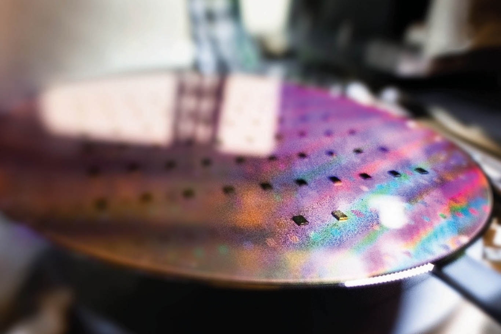
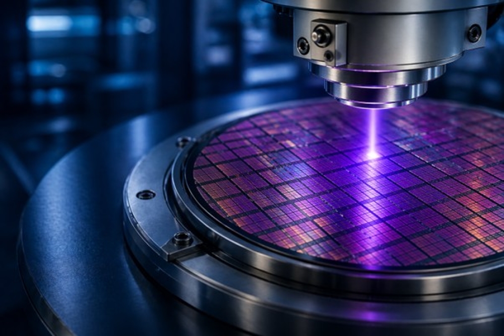
The semiconductor industry is at a pivotal moment. As digital transformation accelerates, driven by artificial intelligence, edge computing, 5G/6G connectivity, and electrification, advanced packaging has moved from being an incremental enhancement to a strategic imperative. Today’s heterogeneous systems, ranging from 2.5D and 3D ICs to fan-out wafer-level packaging (FOWLP), deliver unprecedented performance density, improved power efficiency, and reduced form factors. Yet these benefits come with an unavoidable challenge: Yield pressure.
Yield is no longer merely about defect counts; it’s about understanding how materials behave across scales, interfaces, and processes. Traditional defect inspection methods, while still valuable, are no longer sufficient on their own. The key to unlocking sustainable yield improvements lies in materials-driven failure analysis: a multidisciplinary approach that links material characteristics, structural integrity, process interactions, and comprehensive failure mechanisms into a unified diagnostic framework.
This article examines how materials science, advanced characterization, cross-functional collaboration, and predictive analytics converge to identify hidden failure drivers, enhance process accuracy, and deliver measurable gains in advanced packaging yield.
Why yield matters more than ever in advanced packaging
Advanced packaging technologies, including FOWLP, 3D TSV stacks, chiplets, and integrated passive devices, are increasingly used to meet the demand for higher performance and smaller footprints. These approaches promise reduced interconnect length, improved signal integrity, and enhanced thermal performance. But they also introduce complex materials interfaces, thermal stresses, and multi-physics interactions that are highly sensitive to process variability.
In traditional packaging, yield problems could often be
traced to specific process steps. In advanced packaging, yield excursions can
originate from subtle variations in material properties, interfacial
degradation, or microscale stress accumulationthat may not be readily
observable with optical or electrical inspection alone.
The economic implications are significant. Yield
improvements directly influence usable wafer output, which in turn affects
revenue per wafer, cost of goods sold (COGS), and profitability. Even small
incremental yield gains in high-value advanced packages can generate
substantial financial returns.
This is where materials-driven failure analysis becomes indispensable: it transforms yield investigation from reactive troubleshooting into a proactive engineering discipline.
What materials-driven failure analysis actually means
At its core, materials-driven failure analysis is the
systematic investigation of failure modes through the lens of materials
behaviour and interactions. Rather than simply identifying that a failure
occurred, this approach seeks to understand why it occurred at a fundamental
level:
- What specific material property variations contributed to the defect?
- How did interfacial stress accumulate under processing conditions?
- Did thermal expansion mismatch cause microcracking or delamination?
- Were contamination or
unintended residue responsible for
electrical anomalies?
In advanced packaging, these questions often revolve around
a handful of recurring themes:
- Interfacial integrity: Particularly between dielectrics, metal interconnects, solder joints, and underfill materials.
- Thermo-mechanical stress: From thermal cycling during reflow and operation, especially in stacked components.
- Material anisotropy: Variations in material properties depending on orientation or deposition method.
- Environmental susceptibility: Moisture ingress and electromigration in dense interconnect networks.
Materials-driven analysis involves correlating microscale material behavior with macroscale system performance. It assumes that to improve yields at scale, engineers must first understand the underlying multiscale physics.
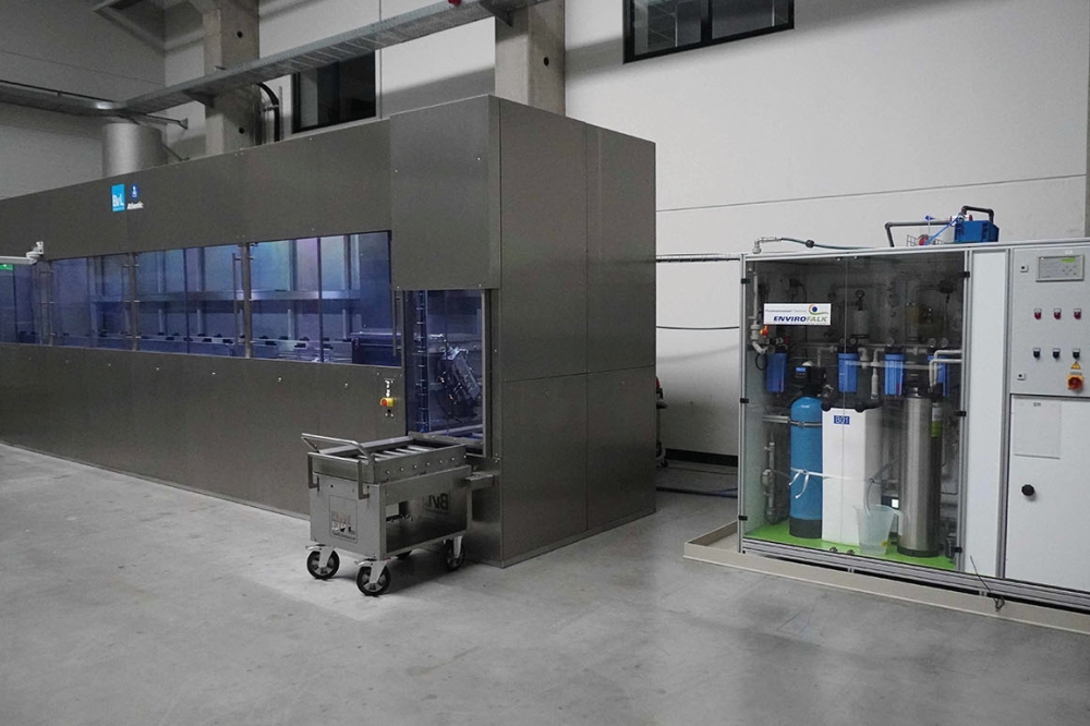
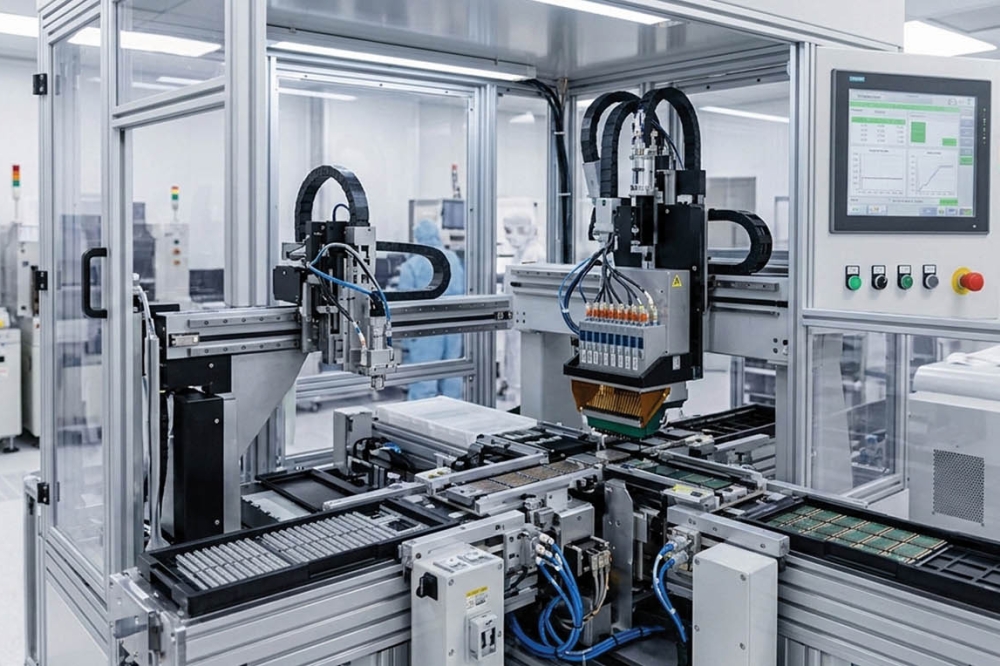
Bringing the right tools to the investigation
To implement materials-driven failure analysis,
organisations must expand beyond conventional electrical tests and optical
inspection. Modern failure analysis blends multiple characterization
techniques:
- Electron
Microscopy and X-ray Imaging
Scanning electron microscopy (SEM), focused ion beam (FIB) cross-sectioning, and X-ray computed tomography (XCT) enable visualization of sub-micron defects, voids in solder joints, delamination, and dielectric cracking. These tools reveal structural anomalies that are invisible in traditional 2D microscopes. - Nanoindentation
and Mechanical Property Mapping
These methods provide insights into local stiffness, hardness, and modulus variations, particularly at interfaces where materials with differing elastic properties meet. Mapping these mechanical gradients helps identify stress concentration zones prone to failure. - Thermal
Imaging and Infrared Thermography
Because advanced packages often suffer from localized heating, thermal imaging helps pinpoint hotspots and thermal patterns that correlate with material degradation or poor thermal conduction paths. - Elemental
and Phase Analysis
Techniques such as energy-dispersive X-ray spectroscopy (EDS) and electron backscatter diffraction (EBSD) reveal compositional variations, grain orientation, phase transformations, and unintended inclusions all of which influence reliability. - In-situ
Stress/Strain Measurement
Advanced optical and X-ray-based methods enable stress mapping during thermal cycling or mechanical loading, providing a direct correlation between process conditions and material responses.
By combining these tools into an integrated workflow, engineers can transform raw data into actionable insight.
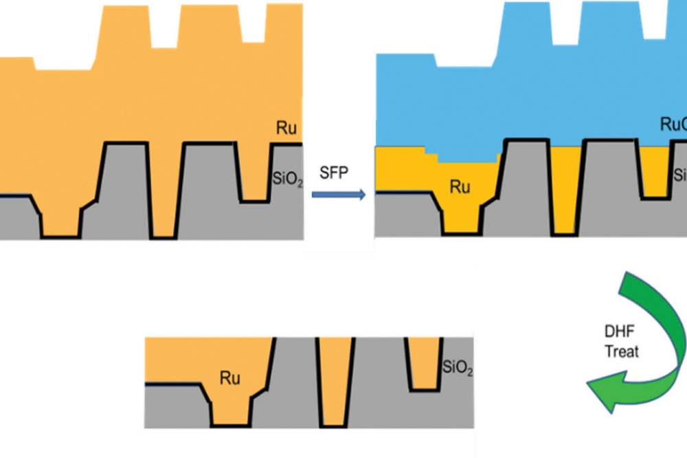
Case study: Interfacial delamination in a 3D package
Consider a common failure mode of advanced packages:
interfacial delamination between an organic substrate and a redistributed layer
(RDL). On the surface, delamination appears as an area of poor adhesion
detectable through acoustic microscopy. But mixed materials analysis often
reveals the root cause lies in:
- A mismatch in the coefficient of thermal expansion (CTE) between layers
- Micro-scale voids generated during lamination
- Localised moisture trap
points exacerbate thermal stress
Materials-driven analysis might proceed as follows:
- Thermo-mechanical modelling identifies zones of highest mechanical stress under reflow and service conditions.
- Nanoindentation and modulus mapping detect unexpected stiffness gradients near the interface.
- XCT imaging reveals micro-void clusters that act as stress concentrators.
- EDS analysis uncovers
contamination or residue at the
interface that reduced adhesion strength.
With this information, engineers can adjust the substrate prep process, revise laminate materials, or modify reflow profiles to minimise stress buildup — leading to measurable yield improvements.
This kind of diagnostic precision is only possible when material behavior is the starting point, not an afterthought.
Materials databases and predictive analytics
Modern yield improvement practices increasingly incorporate materials databases and predictive models. By cataloguing materials properties, including modulus, thermal conductivity, moisture uptake, and ageing behaviour, organizations can develop multi-factor predictive models that estimate failure probability under given process conditions.
Machine learning tools can also be employed to detect patterns in historical failure data, linking material signatures to defect types. For example, correlating shifts in specific viscoelastic properties with increased solder joint fatigue can pre-emptively flag future yield risks.
These data-driven methods reduce reliance on iterative trial-and-error and accelerate actionable insight across design, engineering, and production teams.
Collaborative failure analysis workflows
High-volume manufacturing environments benefit from integrating failure analysis into cross-functional workflows. Materials insights must be communicated upstream to design and process engineers, and downstream to production teams. A robust feedback loop ensures that lessons from failure analysis directly influence design rules and process controls.
Increasingly, organisations are standardising failure reporting and remediation frameworks, enabling accountability and trend identification at enterprise scale.
Collaborative platforms unify data from lab analysis, field
returns, reliability testing, and statistical process control, creating a
closed-loop system of continuous improvement.
Execution challenges and cultural shifts
Materials-driven failure analysis is not simply a set of
tools; it is a mindset. Organisations that excel in yield improvement cultivate
a culture where:
- Engineers
embrace multidimensional investigation, not
one-dimensional metrics
- Materials science is treated as a core competency, not a peripheral function
- Cross-disciplinary dialogue is encouraged between materials, reliability, process, and design teams
Investing in analytical infrastructure and talent is part of this shift, but so is enabling domain expertise to evolve through applied learning rather than rote troubleshooting.
Benefits beyond yield
The value of materials-driven yield improvement extends
beyond defect reduction. Organisations that understand their materials at a
fundamental level benefit from:
- More predictable process windows
- Reduced time-to-market for new packages
- Higher confidence in reliability performance
- Fewer field failures and warranty costs
- Better readiness for next-gen materials like low-k dielectrics, novel underfills, and heterogeneous substrates
The approach builds resilience into the entire product lifecycle, from research to mass production to service.
Conclusion: A new imperative for advanced packaging
Advanced packaging is indispensable for meeting future compute, connectivity, and power requirements. Yet without a deliberate focus on materials behavior and failure mechanisms, yield challenges will remain a primary barrier to scalability and profitability.
Materials-driven failure analysis offers a systematic, multidisciplinary framework for understanding why defects occur, how they propagate, and what conditions exacerbate them. By leveraging advanced characterization, predictive analytics, and collaborative workflows, organisations unlock yield not as a temporary improvement but as an ongoing engineering discipline.
In an era when performance expectations are high and process
margins are tight, the differentiator will not be inspection alone, but insight
- insight into material behaviour, interface integrity, and how the tiniest
anomalies can create the biggest impacts.