MIRPHAB: Sensor boutique for early adopters

Every chemical substance absorbs a very individual fraction of infrared light. Like a human fingerprint, this absorption can be used with optical methods for identifying substances. Such methods are used in the chemical industry, for example, but also in the health sector or in criminal investigation. If a company plans a new project, it often needs individually tailored sensor solutions. In the search for a suitable system, they are now supported by the EU-funded pilot line MIRPHAB (Mid InfraRed PHotonics devices fABrication for chemical sensing and spectroscopic applications) for the development of sensor technology and measurement technology in mid-infrared (MIR). Three Fraunhofer institutes are participating in this project.
If a company is looking for a sensor solution, such as to identify a certain substance in the production process, it often has very individual requirements. This starts with the substances to be accounted for to the number of required sensors up to the speed of the production process. In most cases, a »one-size-fits-all« solution is not sufficient, and several suppliers are needed to develop the optimal individual solution. This is where MIRPHAB comes in: In the pilot line, leading European research institutes and companies from the MIR environment have joined forces to provide customers with tailor-made offers from a single source. Interested parties can address a central contact person, who then compiles the best possible solution from the component portfolio of the MIRPHAB members according to the modular principle.
In order to strengthen the European industry in the long term and expand its leading position in chemical analysis and sensor technology, the development of the individual MIR sensor solutions within the framework of MIRPHAB is supported by EU funding. This significantly reduces the investment costs and, thereby, the entry threshold for companies in the MIR area. In combination with the virtual infrastructure which has been developed during MIRPHAB, high-quality MIR sensor solutions are therefore also of interest to companies for whom the costs and development efforts have previously been seen as being too high. In addition, MIRPHAB gives companies access to the latest technologies, enabling them to gain an edge over the competition as an early adopter.
Customized MIR laser source
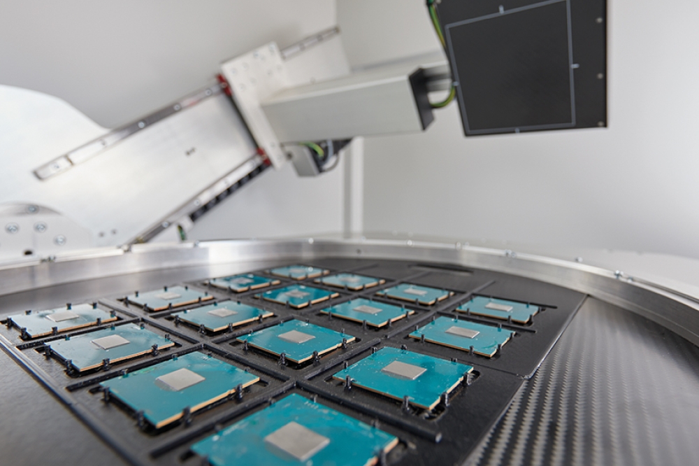
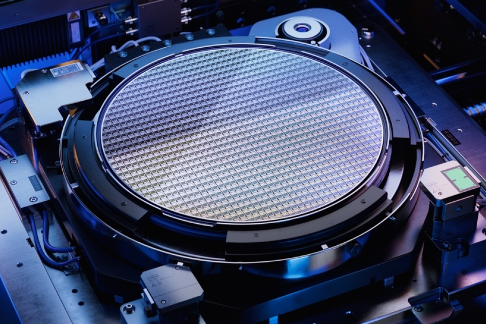
A central component of the MIRPHAB sensor solutions is being provided by the Fraunhofer Institute for Applied Solid State Physics IAF in Freiburg in cooperation with the Fraunhofer Institute for Photonic Microsystems IPMS in Dresden. The Fraunhofer IAF is introducing the technology of quantum cascade lasers, which emit laser light in the MIR range. In this type of laser, the wavelength range in which the light is emitted is spectrally very broad and can be customized during manufacturing. In order to select a specific wavelength within the wide spectral range, it has to be chosen via an optical diffraction grating and coupled back into the laser chip. By rotating the grating, the wavelength can be tuned continuously. The grating is produced at the Fraunhofer IPMS in miniaturized form in so-called Micro-Electro-Mechanical-System (MEMS) technology. This makes it possible to oscillate the grating at a frequency of up to one kilohertz and to thereby tune the wavelength of the laser source up to a thousand times per second over a very wide spectral range.
The Fraunhofer Institute for Production Technology IPT in Aachen is also involved in MIRPHAB in order to make the production of lasers and gratings more efficient and to optimize them for pilot series production. With its expertise, it transforms the production of the rapidly-tunable MIR laser into industrially applicable production processes.
Process analysis in real time
At present, numerous applications in the field of spectroscopy are still in the visible or near infrared range and use relatively weak light sources. MIRPHAB offers solutions based on infrared semiconductor lasers. These have a significantly higher light intensity, thereby enabling completely new applications. As a result, up to 1,000 spectra per second can be recorded with the MIR laser source, which, for example, enables the automated monitoring and control of chemical reactions and biotechnological processes in real time. MIRPHAB is therefore making an important contribution to the factory of the future and Industrie 4.0.