Imec and Cascade Microtech Develop First Automatic Probe System for Advanced 3D Chips

Imec, leading research and innovation hub in nano-electronics and digital technologies, and Cascade Microtech, a FormFactor company in advanced wafer-probe solutions, has announced the successful development of a fully-automatic system for pre-bond testing of advanced 3D chips. Pre-bond testing is important to increase the yield of 3D stacked chips. The new system enables probing and hence testing of chips with large arrays of 40 µm-pitch micro-bumps, on 300 mm wafers. The relevance of this new tool is underlined by winning the 2017 National Instruments Engineering Impact Award yesterday at a ceremony in Austin, Texas.
As an emerging technology, 3D IC stacking still has many open options and technical challenges. One of these challenges is probing of the individual chips, before being stacked, to ensure a good yield of the 3D stacked ICs. The inter-chip connections of 3D stacked ICs are made by large arrays of fine-pitch micro-bumps which makes probing these bumps a challenge. Until today, the probing solution is to add dedicated pre-bond probe pads to the to-be-stacked dies, but this requires extra space and design effort and increases test time.
Imec and Cascade Microtech have now developed a fully automatic test cell that can provide test access by probing large arrays of fine-pitch micro-bumps. The system is based on a Cascade Microtech CM300 probe station and National Instruments PXI test instrumentation, complemented by in-house developed software for automatic test generation, data analysis, and visualization. The system allows testing of wafers up to 300mm diameter, including thinned wafers on tape frame with exposed through-silicon vias. After several years of intense collaboration between imec and Cascade Microtech, partly supported by the EU-funded FP7 SEA4KET project, good results were achieved with Cascade Microtech's Pyramid Probe® prototype RBI probe cards on imec's 300 mm wafers with 40µm-pitch micro-bumped chips.
"Imec provided us with unique early insights into the test requirements for 3D ICs, which drove the development of this system," said Jörg Kiesewetter, director of engineering at Cascade Microtech Dresden. "Also the availability of imec's dedicated micro-bump test wafers has helped us to fine-tune both the probe station and the probe cards for this application."
"At imec, we are using the system now on a routine basis to test our 40µm-pitch micro-bumped wafers," stated Erik Jan Marinissen, principal scientist at imec. "As everything in the semiconductor realm, also micro-bumps are subject to downscaling. Hence, with Cascade, we have started experiments to also probe our 20µm-pitch micro-bump arrays, and those look promising."

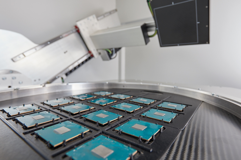
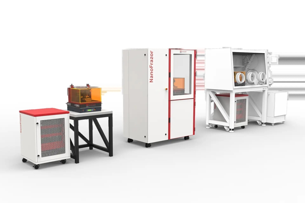
Figure 1 "“ The test system as installed in imec's Fab-2.
 Â
Â
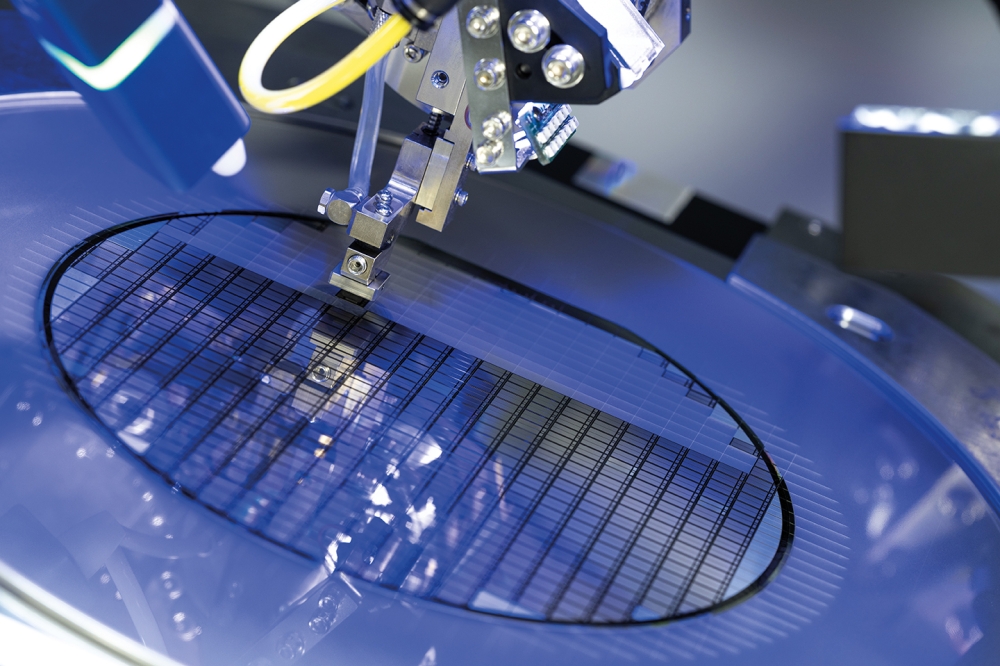
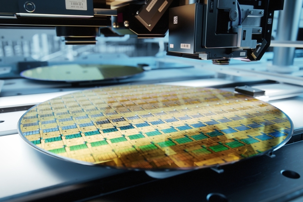
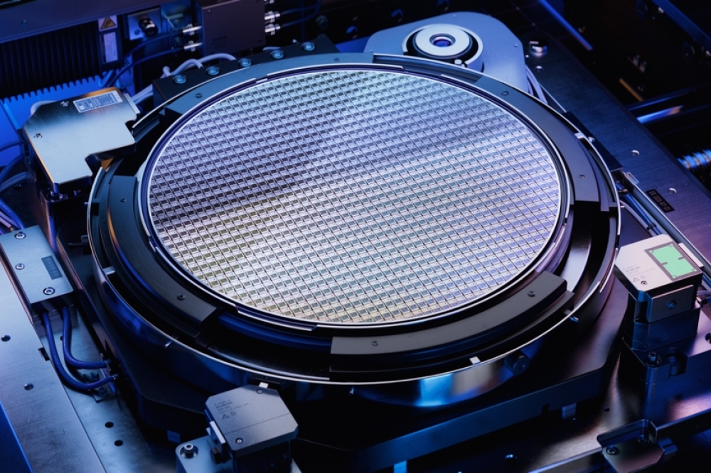
Figure 2 "“ At the heart of the test system is this probe core with MEMS-based probe tips that contact the large arrays of fine-pitch micro-bumps.
Â