Unisem Selects Two Veeco Tools to Support Expansion of FOWLP

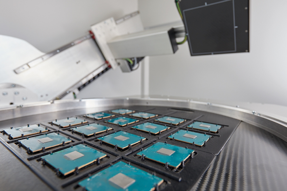
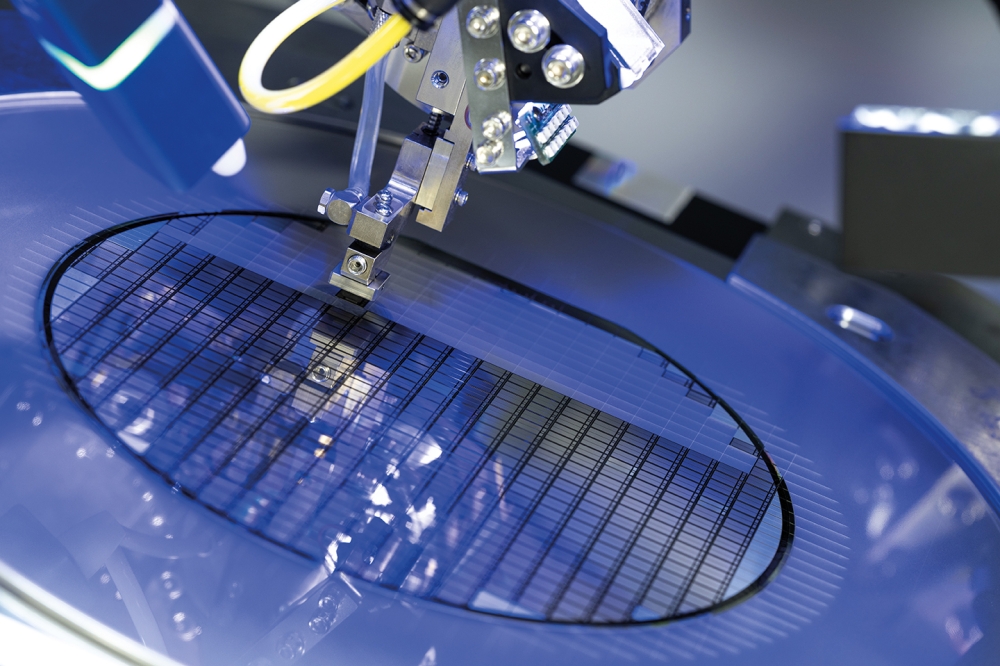
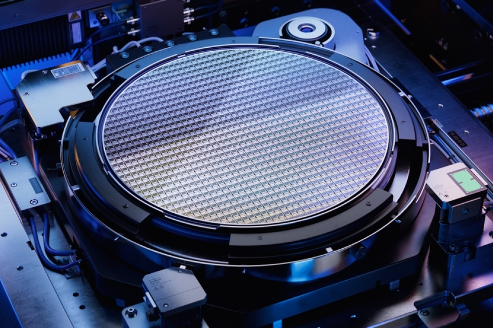
Veeco Instruments has announced that Unisem Advanced Technologies Sdn Bhd (UAT) has purchased Veeco’s WaferStorm single wafer solvent wet process tool and its AP300 lithography system to support the growth of its outsourced assembly and test (OSAT) business. One of the first independent wafer bumping service providers in Malaysia, UAT will leverage these tools for services including gold, electroplated solder and electroplated copper pillar bumping as it expands fab capacity from 8-inch to 12-inch platforms necessary for progressive fan-out wafer-level packaging (FOWLP) applications.
“FOWLP techniques have proven critically important for improving electrical and thermal performance in the bumping process,” said Chan Wah Chai, general manager at UAT. “We’re excited to forge this new partnership with Veeco and are confident our adoption of the WaferStorm and AP300 tools will support our efforts to enable next-generation packaging techniques leveraging fan-out technology.”
While advanced techniques such as FOWLP and 3D integration comprise less than 10 percent of the market today, they are predicted to grow at over 15 percent CAGR over the next few years. According to TechSearch, the demand for wafers incorporating FOWLP will grow from 1 million wafers per year in 2018 to more than 6 million wafers per year in 2021.
“It’s increasingly evident that advanced packaging is an enabler to better performance in high-potential, high-growth applications such as artificial intelligence and autonomous vehicles,” said Scott Kroeger, vice president and general manager of Veeco’s Precision Surface Processing business unit. “As packaging designs like FOWLP gain momentum, customers require better process control, advanced resist removal technologies for smaller dimensions and low chemical consumption to competitively scale these devices. We are proud to be working with companies like UAT who expect higher standards to deliver on their customer promises and are confident that WaferStorm will help the industry achieve high-performance standards at low cost of ownership.”
WaferStorm is a solvent-based single wafer wet process platform that deploys Veeco’s unique ImmJET technology at its core. ImmJET delivers repeatable performance for the industry’s toughest applications at lower cost of ownership than conventional batch or spray-only approaches. WaferStorm offers proven, reliable solutions for metal lift-off, photoresist strip, dry film resist strip, via cleans, flux removal and other advanced processes.
The AP300 lithography system is built on Veeco’s customizable Unity Platform, delivering a winning combination of overlay, resolution and side wall profile performance and enabling highly automated and cost-effective manufacturing. The AP300 system is particularly well suited for copper pillar, fan-out, through-silicon via and silicon interposer applications.
“While FOWLP offers advantages like smaller form factors and heterogeneous integration of diverse die types, there are still challenges from a lithography standpoint when it comes to performance and yield,” added Peter Porshnev, senior vice president and general manager of Veeco’s Ultratech business unit. “The AP300 tool provides a robust lithography solution for the challenging FOWLP processes required to manufacture high-performance next-generation devices.”