Renesas Invest and Restart Operation of Kofu Factory

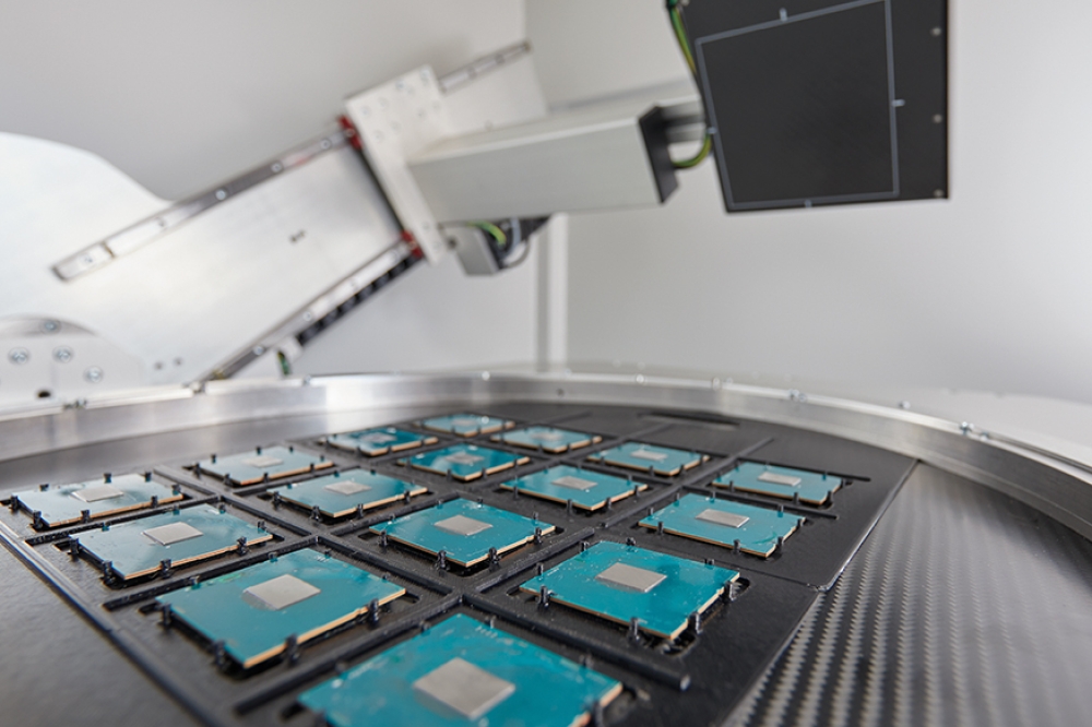
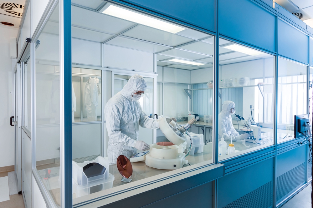
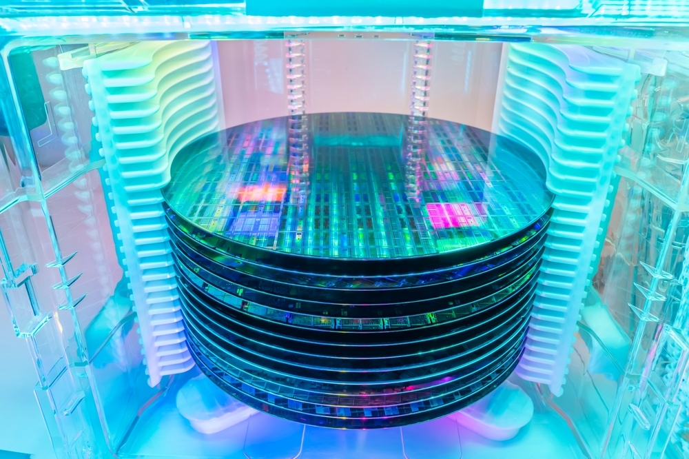
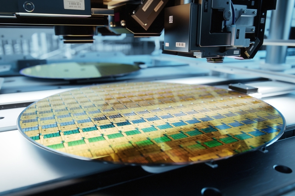
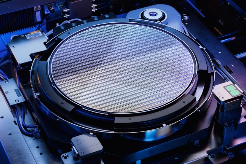
Renesas Electronics, a supplier of advanced semiconductor solutions, has announced that it will conduct a 90-billion-yen worth investment in its Kofu Factory, located in Kai City, Yamanashi Prefecture, Japan. While the Factory was closed in October 2014, Renesas intends to reopen the fab in 2024 as a 300-mm wafer fab capable of manufacturing power semiconductors.
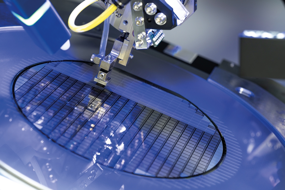
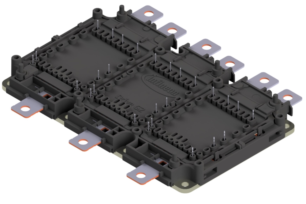
As the momentum for carbon neutrality grows, demand for highly efficient power semiconductors, which supply and manage electricity, is expected to dramatically increase globally over the years. Renesas especially anticipates rapid growth in demand for electric vehicles (EVs), and therefore plans to enhance its production capacity for power semiconductors such as IGBTs, in order to contribute toward decarbonization. Once the Kofu Factory reaches its mass production, the total production capacity of Renesas’ power semiconductors will double.
The Kofu Factory of Renesas Semiconductor Manufacturing Co., Ltd., a wholly-owned subsidiary of Renesas, previously operated both 150mm and 200mm wafer fabrication lines. To boost its production capacity, Renesas decided to utilize a remaining building of the factory and revive it as a 300mm wafer fab dedicated to power semiconductors.
“Sustainability is at our heart and with ‘To Make Our Lives Easier’ as our Purpose, we want to build a sustainable future where our semiconductor technology and solutions help make our lives easier,” said Hidetoshi Shibata, President and CEO of Renesas. “This investment enables us to have our largest wafer fabrication line dedicated to power semiconductors, which are key to realizing decarbonization. We will continue to conduct necessary investments to enhance our in-house production capability while further strengthening ties with outsource partners. To address the mid to longer term demand growth, Renesas remains committed to ensuring security of supply in order to provide our customers with the best possible support.”
With the Japanese Ministry of Economy, Trade and Industry’s Strategy for Semiconductors in consideration, Renesas plans to conduct its investment within the year of 2022, while closely coordinating with the Ministry.
While this investment will not have a material impact on Renesas’ performance for the year of 2022, an announcement will be promptly issued if, following this investment, any material impact is made.