TSMC holds 3nm volume production and capacity expansion ceremony

Marks a key milestone for advanced manufacturing.
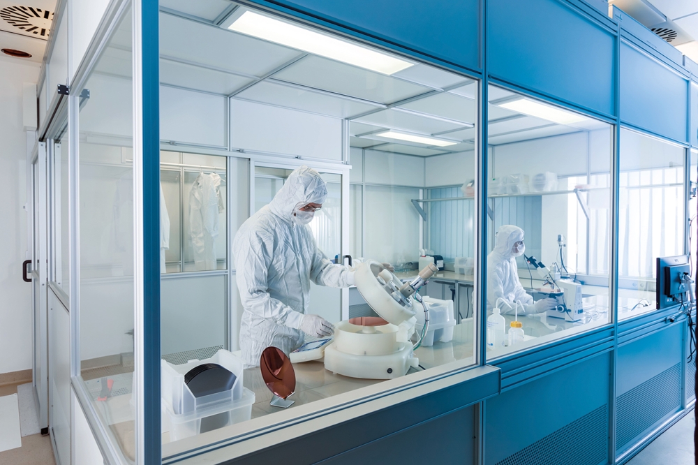
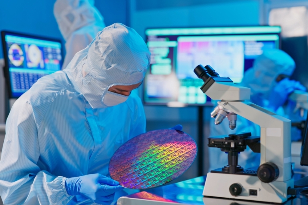
TSMC has held a 3 nanometer (3nm) Volume Production and Capacity Expansion Ceremony at its Fab 18 new construction site in the Southern Taiwan Science Park (STSP), bringing together suppliers, construction partners, central and local government, the Taiwan Semiconductor Industry Association, and members of academia to witness an important milestone in the Company’s advanced manufacturing.
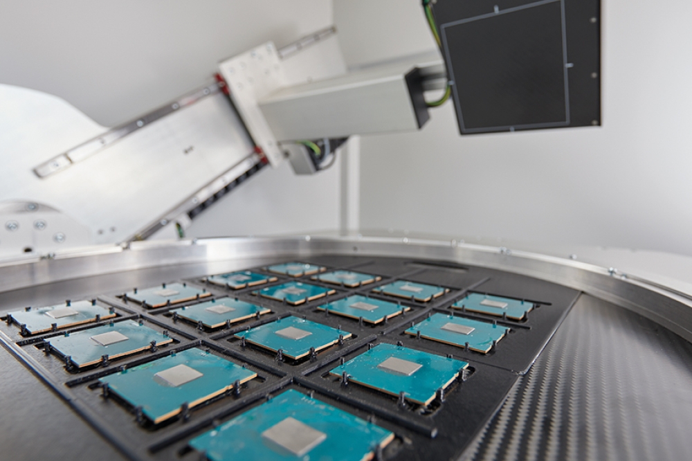
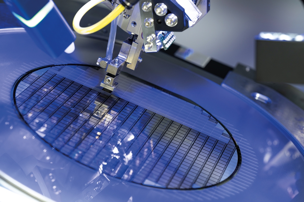
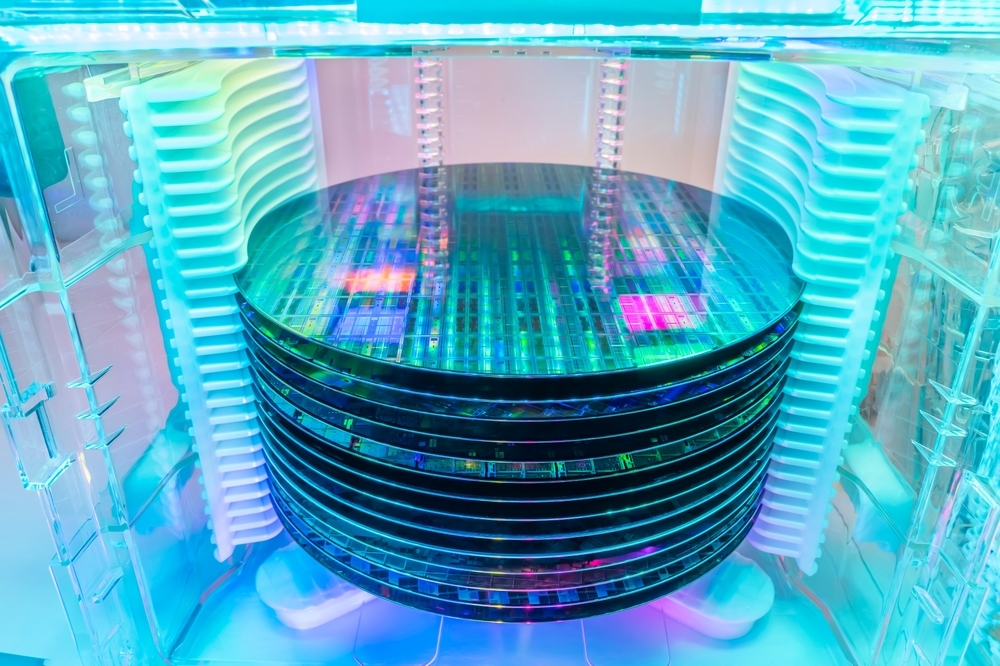
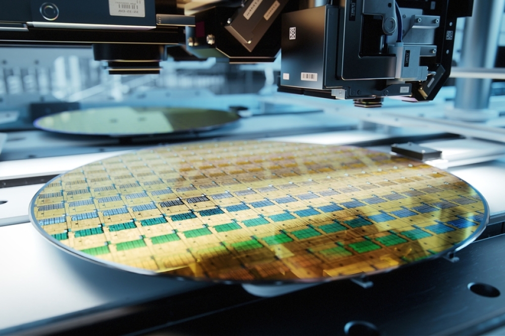
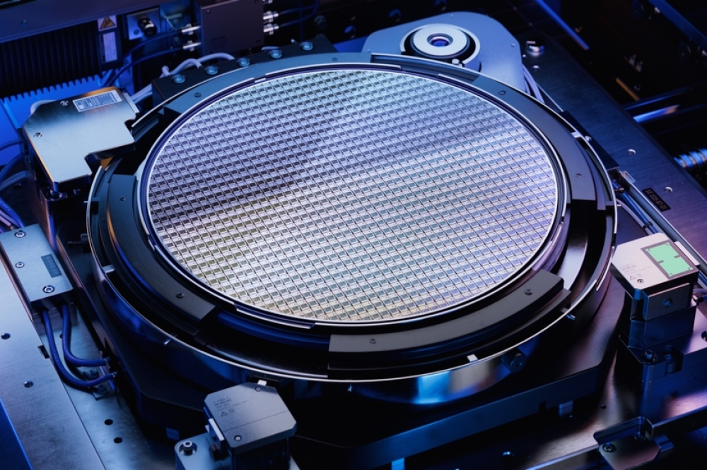
TSMC has laid a strong foundation for 3nm technology and capacity expansion, with Fab 18 located in the STSP serving as the Company’s GIGAFAB® facility producing 5nm and 3nm process technology. Today, TSMC announced that 3nm technology has successfully entered volume production with good yields, and held a topping ceremony for its Fab 18 Phase 8 facility. TSMC estimates that 3nm technology will create end products with a market value of US$1.5 trillion within five years of volume production.
Phases 1 through 8 of TSMC Fab 18 each have cleanroom area of 58,000 square meters, approximately double the size of a standard logic fab. TSMC’s total investment in Fab 18 will exceed NT$1.86 trillion, creating more than 23,500 construction jobs and over 11,300 high-tech direct job opportunities. In addition to expanding 3nm capacity in Taiwan, TSMC is also building 3nm capacity at its Arizona site.
TSMC also announced that the Company’s global R&D Center in the Hsinchu Science Park will officially open in the second quarter of 2023, to be staffed by 8,000 R&D personnel. TSMC is also making preparations for its 2nm fabs, which will be located in the Hsinchu and Central Taiwan Science Parks, with a total of six phases proceeding as planned.
TSMC Chairman Dr. Mark Liu presided over 3nm Volume Production and Capacity Expansion Ceremony, and notable guests at the event included Vice Premier Shen Jong-chin, Minister of Economic Affairs Wang Mei-hua, Minister of Science and Technology Wu Tsung-tsong, Tainan City Mayor Huang Wei-che, STSP Administration Bureau Director-General Su Chen-kang, Fu Tsu Construction Chairman Cliff Lin, United Integrated Services Chairman Belle Lee, National Cheng Kung University President Dr. Jenny Su, Chang Chun Petrochemical President Chih-Chuan Tsai, Kuang Ming Enterprise Co. Vice Chairman Eric Lin, and Applied Materials Group Vice President Erix Yu, as well as representatives from TSMC’s construction partners, materials and equipment suppliers, the Taiwan Semiconductor Industry Association and academic institutions.
“TSMC is maintaining its technology leadership while investing significantly in Taiwan, continuing to invest and prosper with the environment. This 3nm Volume Production and Capacity Expansion Ceremony demonstrates that we are taking concrete action to develop advanced technology and expand capacity in Taiwan,” TSMC Chairman Dr. Mark Liu said at the ceremony. “We aim to grow together with our upstream and downstream supply chain and develop future talent from design to manufacturing, packaging and testing, equipment, and materials to provide the most competitive advanced process technology and reliable capacity for the world and drive technology innovation in the future.”
TSMC is committed to flourishing with the natural environment through green manufacturing, and all of TSMC’s construction in the STSP follows Taiwan’s EEWH and the U.S. LEED green building certification standards. The facilities will also use water resources from the TSMC STSP Reclaimed Water Plant to gradually reach the company’s target of using 60% reclaimed water by 2030. Once volume production begins, Fab 18 will use 20% renewable energy to eventually reach the sustainability goal of 100% renewable energy and zero emissions by 2050.
TSMC’s 3nm process is the most advanced semiconductor technology in both power, performance, and area (PPA) and in transistor technology, and a full-node advance from the 5nm generation. Compared with the 5nm (N5) process, TSMC’s 3nm process offers up to 1.6X logic density gain and 30-35% power reduction at the same speed, and supports the innovative TSMC FINFLEX™ architecture.