Keysight acquires Cliosoft
Acquisition to digitally transform design-test workflows and meet productivity requirements of next-generation electronic product development lifecycles.
Keysight Technologies has acquired Cliosoft and will be adding the company’s line of hardware design data and intellectual property (IP) management software tools to its portfolio of electronic design automation (EDA) solutions.
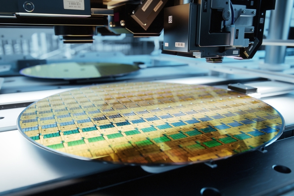
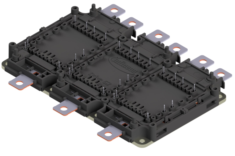
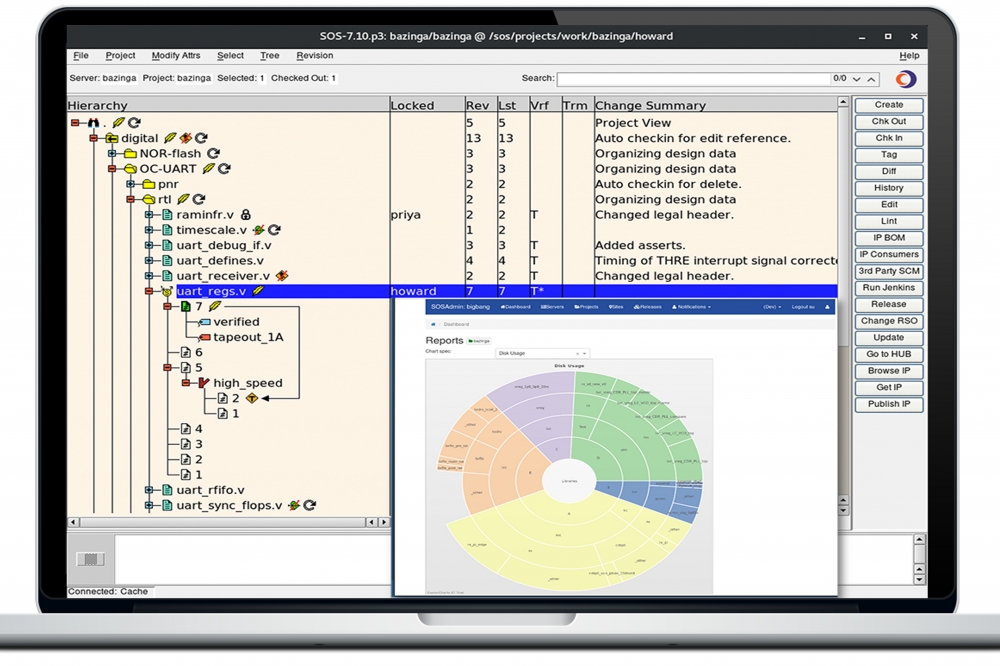
Since its inception, Cliosoft’s primary focus has been managing design data, including functional IP blocks used in integrated circuits. Cliosoft’s products expand Keysight’s EDA software offering to include process and data management (PDM) capabilities that have been adopted by more than 400 global semiconductor and electronics systems customers.
By bringing Cliosoft into its EDA business, Keysight boosts its intelligent automation software offerings with PDM as an essential component in building the foundation for more productive workflows. Keysight is extending Cliosoft’s capabilities to include test data in a fabric that provides customers with a much stronger link between design and test.
Keysight and Cliosoft are long-standing industry collaborators as Cliosoft SOS, a data management platform, already integrates with Keysight’s Advanced Design System (ADS) solution which many mutual customers currently use. The combined companies will continue to offer revision control and data and IP management solutions through EDA industry relationships, including Cadence, Empyrean, MathWorks, Siemens EDA, Silvaco, and Synopsys environments.
Keysight and Cliosoft share the philosophy that PDM is critical to first pass success of customer designs in global engineering enterprises. Design complexity is expanding the volume of IP blocks and data that engineering teams must effectively and efficiently manage. Industry trends such as heterogeneous integration, advanced packaging, and 24x7 follow-the-sun research and development operations are driving customers towards the next level of productivity improvements.
Niels Faché, Vice President and General Manager of Keysight EDA, said: “One of our top business priorities is creating digital, connected workflows from design to test that accelerate customers’ digital transformation. We see a tremendous opportunity in the PDM space to leverage Cliosoft’s current capabilities combined with our design-test solutions expertise. Adding PDM solutions to the portfolio is a natural progression of our open EDA interoperability strategy to deliver best-in-class tools and workflows in support of increasingly complicated product development lifecycles. Cliosoft offers proven software tools that enable product teams to perform data analytics and accelerate time to insight. The result of faster insight and greater reuse is improved productivity in the verification phase and shorter overall development cycles.”
Srinath Anantharaman, Chief Executive Officer of Cliosoft, added: “Handling exponential growth in design data and maximizing IP reuse with interoperability across EDA vendor environments is a major challenge as we approach the time of ‘More than Moore’s law’. Keysight’s broad industry leadership in applications like 5G and 6G communications, automotive, and aerospace and defense, makes Keysight uniquely positioned to realize the promise of connecting design, emulation, and test data in streamlined workflows that speed time-to-market. We are excited to join Keysight in raising engineering productivity to the next level and enabling our customers to digitally transform their development lifecycles and meet the challenges ahead.”