+44 (0)24 7671 8970
More publications     •     Advertise with us     •     Contact us
 
Loading...
News Article

KIOXIA’s major new sustainability initiative

News

KIOXIA installs Solar Power Generation Systems at Kitakami and Yokkaichi Plants in Japan.

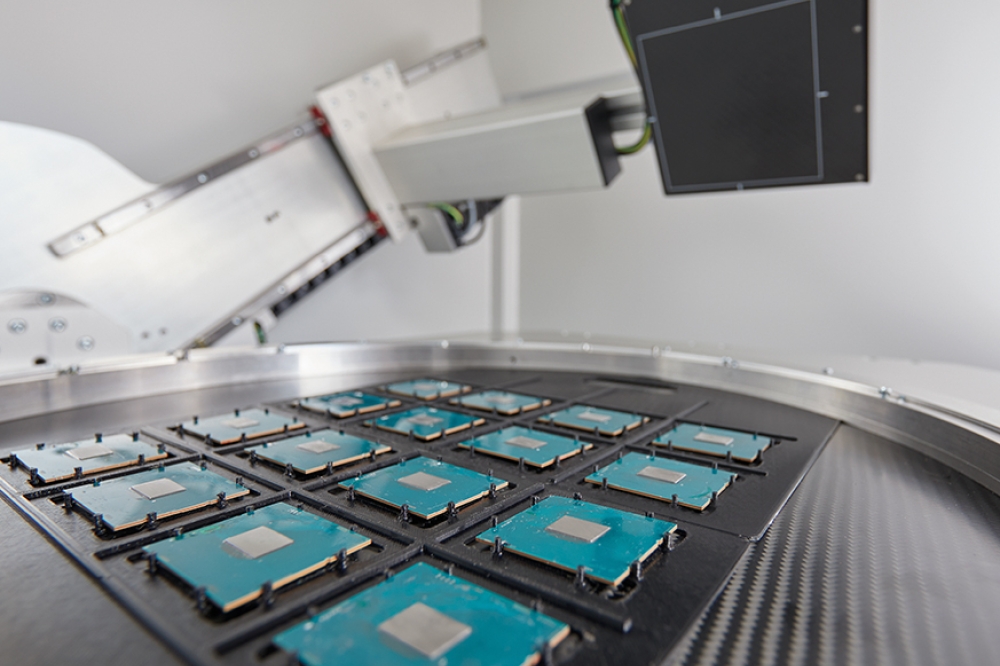
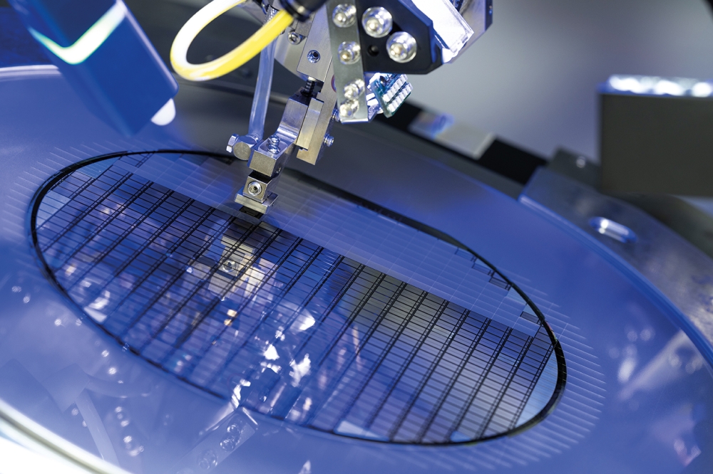
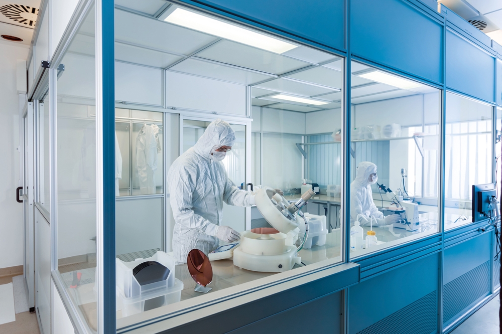
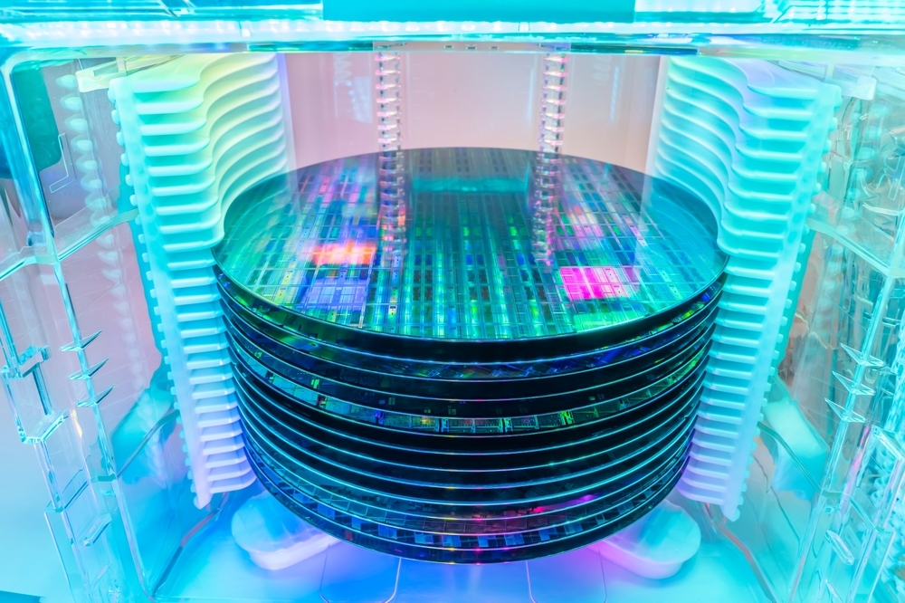
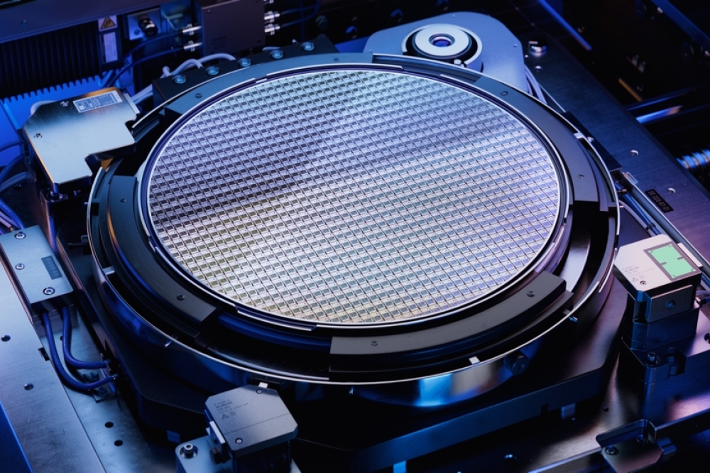
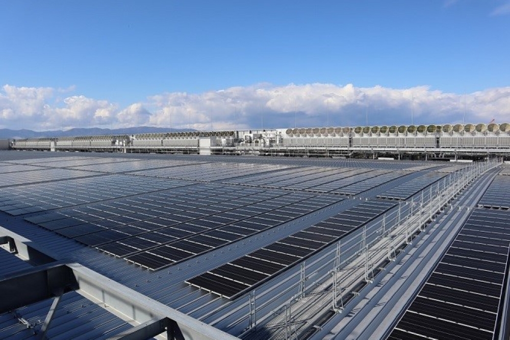
KIOXIA Europe GmbH says that KIOXIA Group is increasing the usage of renewable energy by installing large-scale solar power generation systems for the first time at its Kitakami Plant and Yokkaichi Plant.


Installed on the rooftop of flash memory fabrication facilities, the new solar power systems will be the largest of their kind at any semiconductor plant in Japan. With a total generating capacity of about 7.5 megawatts (MW), the new solar power systems are expected to generate about 7,600 megawatt hours (MWh) of electricity annually for KIOXIA and reduce carbon dioxide emissions by about 3,200 tons per year.


“With the new solar power systems, we will accelerate our efforts to address climate change, one of the key objectives of our management strategy,” explains Asayuki Nannichi, president of KIOXIA Europe GmbH. “The solar power generation system at Fab1 of our Kitakami Plant became operational recently, while the system at Fab6 of our Yokkaichi Plant will be operational in June of this year,” he continues.


KIOXIA Group has set the goal of sourcing 100% of its energy from renewable sources by FY2040, including solar power.

Laser focus on Glasgow
Kaman Measuring introduces ThreadChecker
SandBox Semiconductor adds hybrid metrology capabilities
Intel empowers developers to 'Bring AI Everywhere'
Fab renovation: A blue CHIPS investment
Aqua Membranes collaborates with Micron Technology
Brewer Science releases Impact Report 2023
UK semiconductor strategy: A patent attorney’s perspective
Wafer cleaning market to reach US$ 17.2 billion
Solvay signs partnership agreement with Shengjian
ACM cleaning platform targets chiplets industry
Vietnam's thriving semiconductor industry fuels economic resilience
GSA celebrates women's innovation
The need for geofencing to help improve semiconductor IP security
All roads lead to Arizona
Time to celebrate and accelerate diversity, equity and inclusion
Cadence completes acquisition of PHY IP assets from Rambus
Wales joins the European Semiconductor Regional Alliance
Magnachip targets EV market
Greene Tweed: When it can’t fail
Advanced Packaging market Size to reach $66.9 billion by 2032
Inventec and Renesas to develop PoC for automotive gateways
Renesas commences Sequans tender offer
Tower Semiconductor and InnoLight partner
Flanders Semiconductors - a new hub in the heart of Europe
Ambiq wins Demo of the Year Award
Advanced packaging market nears US$90 billion
Intel Foundry Services and Tower Semiconductor reach US foundry agreement
MediaTek develops first chip using TSMC's 3nm Process
Advanced X-ray technology for advanced packaging
New developments in underlayers and their role in advancing EUV lithography
Advanced SAM validates integrity of electrostatic chucks
×
Search the news archive

To close this popup you can press escape or click the close icon.
Logo
×
Logo
×
Register - Step 1

You may choose to subscribe to the Silicon Semiconductor Magazine, the Silicon Semiconductor Newsletter, or both. You may also request additional information if required, before submitting your application.


Please subscribe me to:


You chose the industry type of "Other"

Please enter the industry that you work in: