Loading...
News Article

Mitsubishi Electric to construct new wafer plant

News

Will double previous five-year investment plan to some 260 billion yen through March 2026.

Mitsubishi Electric Corporation will double a previously announced its investment plan to approximately 260 billion yen in the five-year period to March 2026 mainly for constructing a new wafer plant to increase production of silicon carbide (SiC) power semiconductors. Under the plan, Mitsubishi Electric expects to respond to rapidly increasing demand for SiC power semiconductors for electric vehicles as well as expanding markets for new applications that require, for example, low energy loss, high temperature operation or high-speed switching. The plan will also enable Mitsubishi Electric to contribute to the global green-transformation trend toward energy conservation and decarbonization.

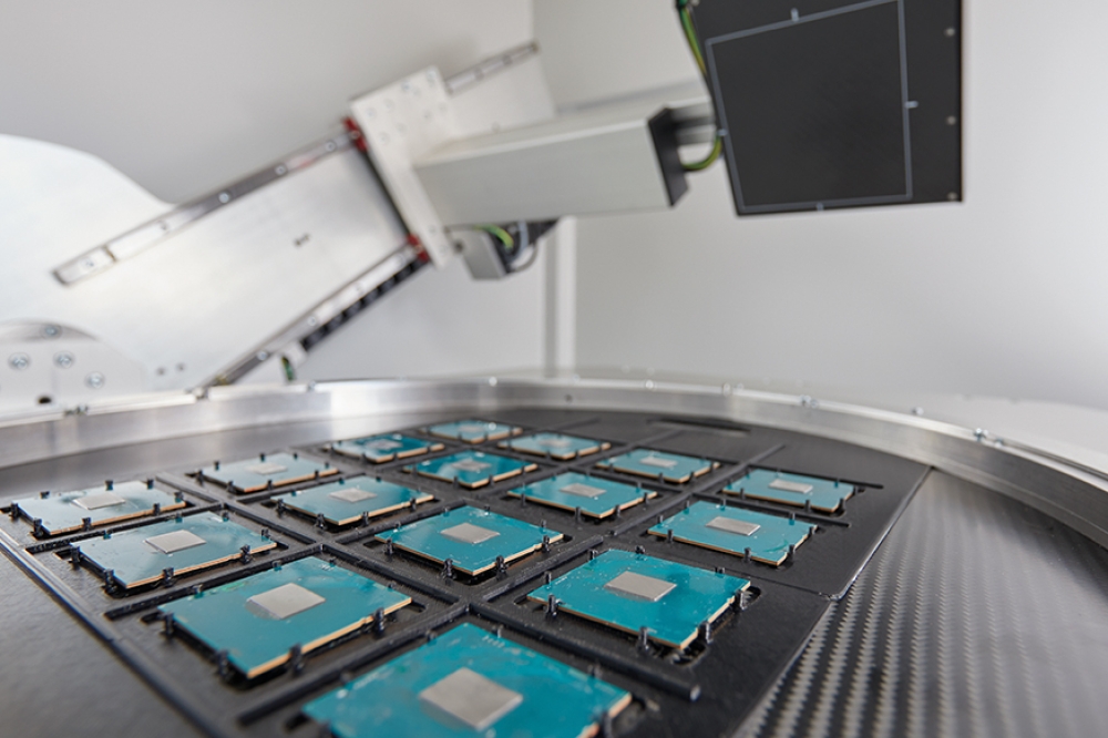
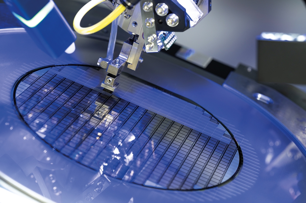
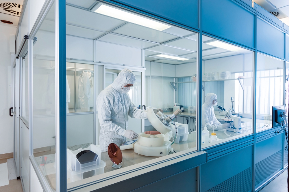
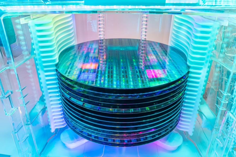
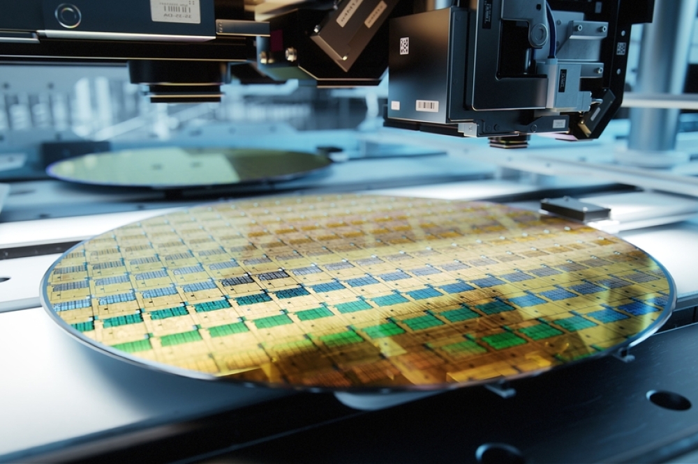
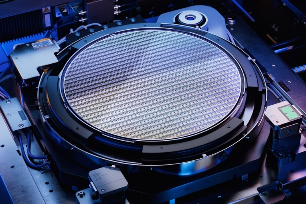
A major portion of the increased investment, approximately 100 billion yen, will be used to construct a new 8-inch SiC wafer plant and enhance related production facilities. The new factory, which will incorporate an owned facility in the Shisui area of Kumamoto Prefecture, will produce large-diameter 8-inch SiC wafers, introduce a clean room featuring state-of-the-art energy efficiency and high-level automated production efficiency. In addition, the company will enhance its production facilities for 6-inch SiC wafers to meet growing demand in this sector as well.

In addition, Mitsubishi Electric will newly invest approximately 10 billion yen in a new factory that will consolidate existing operations, currently dispersed throughout the Fukuoka area, for the assembly and inspection of power semiconductors. The integration of design, development and production technology verification will greatly enhance the company's development capabilities and facilitate timely mass production in response to market demand. The remaining 20 billion yen, all new investment, will be targeted at equipment enhancements, environmental arrangements and related operations.

Next Gen 3D X-Ray Inspection for Advanced Packaging: To see better. Faster. More.
New strategic collaboration between FRAMOS and NXP Semiconductors
Splitting hairs to ten to the power of four
TANAKA introduces “TK-SK” Palladium alloy for test equipment
Rebellions collaborates on next-gen AI computing chiplet technology
Semiconductor giants add $2.7 trillion to their stock values
Test early and test often
Semiconductors: Unstoppable growth in a billion-dollar market
Sustainable cleaning solutions for a greener microelectronics industry
Why the mask world is moving to curvilinear
Beyond AOI: An AI-driven revolution in visual inspection
Xscape Photonics raises $44 million Series A
CMOS sensors for niche vision applications
Emphasis on AI applications
Promoting collaboration and novel IC design technologies
East Asian manufacturer's metrology must-haves
Infineon intensifies sustainability collaboration
Accelerating semiconductor designs for AI applications
Heidelberg Instruments launches nanolithography tool
SEMIFIVE concludes HyperAccel contract
Nova Prism 2 selected by logic manufacturer
Baya Systems expands through partnership with IPro Silicon IP
SensiML and Efabless partner
How to bring photonic chips to the market faster?
Pfeiffer Vacuum becomes Pfeiffer Vacuum+Fab Solutions
Infineon combines silicon and silicon carbide in an e-mobility power module
Jacobs awarded CG Semi contract
Klika Tech joins Nordic Semiconductor Partner Program
Experts warn UK semiconductor firms are at risk from global trade war
Seoul Semiconductor illuminates its wired and wireless networking experience
Amkor and TSMC to expand partnership
Visualisation first for UC Santa Barbara
×
Search the news archive

To close this popup you can press escape or click the close icon.
Logo
x
Logo
×
Register - Step 1

You may choose to subscribe to the Silicon Semiconductor Magazine, the Silicon Semiconductor Newsletter, or both. You may also request additional information if required, before submitting your application.


Please subscribe me to:


You chose the industry type of "Other"

Please enter the industry that you work in: