
Advances in active alignment engines for efficient photonics device test and assembly
The photonics market is advancing rapidly, with projected substantial growth in a large number of sectors incorporating this technology in the next decade. Anticipating devices with hundreds or even thousands of individual components and connections, manufacturers face the necessity of parallel optimization, making active alignment an optimal choice to meet production demands.
By Scott Jordan, Stefan Vorndran and Warren Harvard, Physik Instrumente L.P. (PI)
Over more than a half century, the pace of innovation in electronic communication and computing has consistently increased, giving rise to progressively smaller silicon microchips with enhanced processing power. This achievement is attributed to the exponential growth in the density of integrated circuit (IC) transistors, a development predicted by Gordon Moore, Intel confounder, in 1965 and commonly called Moore’s Law. However, there are inherent limits to reducing the physical feature size of silicon structures before quantum effects start influencing their functionality.
Fortunately, photonics has come to the aid of electronics, enabling the integration of miniaturized optical devices into various applications, from sensors in wearable devices, to LiDAR and ADAS cameras in autonomous vehicles. Photonics has the potential to surpass traditional electronics combining data throughput and efficiency with miniaturization, sparking a true revolution in the telecommunications and data communication sector. To sustain this growth, it is essential to address the remaining challenges and bottlenecks in photonic device manufacturing. The implementation of additional automation solutions, especially those ensuring fast and precise component alignment, is crucial to meet the demands of future advancements.

Optical power distribution of a photonic component and simulated hill-climb algorithm (gradient search). (Image courtesy PI).
Limitations of labor-intensive device assembly
The assembly process of photonic devices typically includes meticulously aligning, gluing, and curing a combination of light sources, fibers, lenses, arrays, waveguides and chips. Each of these individual components must be accurately positioned to ensure the intended functionality and performance of the final product, as even slight misalignments on the orders of less than a millionth of a meter can severely impact device efficiency.
Despite technological advancements, many manufacturers still rely on manual alignment techniques, using shims for error compensation or securing hardware with retaining rings. Beyond being time-consuming, these methods often involve specialized labor that is both costly and challenging to find.
The manual assembly of complex devices can take up to 20 minutes, creating a significant bottleneck in the production process at the component positioning stage. Additionally, traditional assembly tools like shims and jigs may struggle to meet the increasingly stringent tolerances required for manufacturing modern devices. An alternative alignment strategy is necessary to precisely indicate component positioning.

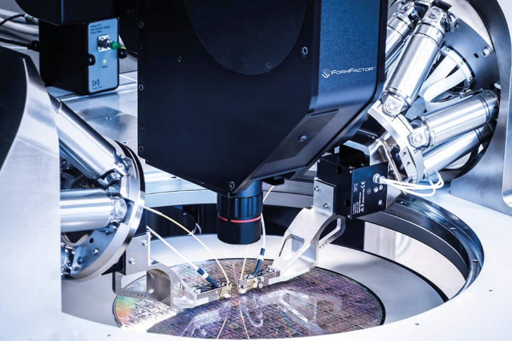
Testing and packaging of modern photonic devices can be a huge challenge
across multiple degrees of freedom. The alignment of multi-channel
devices, such as fiber-optical arrays, used to be a slow, repetitive
process before modern parallel algorithms were developed. (Image
courtesy PI).
Optical feedback to guide automatic alignment engines
A key characteristic of photonic devices is their efficiency’s direct correlation with the alignment of individual components. This means that the output strength dynamically changes in real time with component positions. The varying signal strength serves as a guide for an iterative positional adjustment process, resulting in a precisely aligned assembly. To assess component drift, the fluctuation in photonic output strength can be monitored during the gluing and curing process. However, manually performing this method on complex devices with numerous inputs and outputs becomes impractical. Optimizing one connection can lead to movement affecting others, necessitating constant readjustment for a global consensus. An automated solution is essential to address this challenge, enabling a practical production process that eliminates the need for time-consuming back-and-forth adjustments.
Automating the adjustment process involves closing the feedback loop between device output and positioning hardware, allowing intelligent software solutions and control modules to handle fine-tuning. These systems utilize areal scan algorithms to characterize the assembly, identifying the approximate location of peak photonic output. Multiple gradient searches are then conducted to precisely determine the global optimum. Specialized piezo nano-positioning devices, capable of adjusting several connections simultaneously, guide the components into perfect alignment in an innovative process known as active alignment. Integrated features, including compensation factors, eliminate the need for constant iterative readjustment.
Complete modular solutions are now available, significantly reducing photonic device manufacturing times while maintaining sub-micron precision. Physik Instrumente’s Fast Multichannel Photonic Alignment (FMPA) technology, for instance, can perform multiple alignments, such as in and outputs, across multiple-degrees of freedom, in parallel, reducing assembly time by a factor of 100 or more.

Testing and packaging of modern photonic devices can be a huge challenge across multiple degrees of freedom. The alignment of multi-channel devices, such as fiber-optical arrays, used to be a slow, repetitive process before modern
parallel algorithms were developed. (Image courtesy PI)
Solving the first light capture problem
Since alignment is the top cost driver for photonics device manufacturing, addressing it has been PI’s focus since the award-winning Fast Multichannel Photonics Alignment (FMPA) technologies in 2016. By performing optimization in parallel across multiple channels, components and degrees of freedom and achieving coupling repeatabilities to typically 0.02dB, FMPA reduces the time and cost of manufacturing and testing of photonic devices and improves yield. But before the optimization process can even start, an optical signal, above the noise level, needs to be detectable – this process is called first light capture, and it is particularly time-consuming in devices with inputs and outputs where both sides must be lined up for even a threshold amount of coupling to be achieved. Finding first light has been a time-consuming procedure in all industrial photonics alignment applications, including wafer probing and device packaging.

A PILightning-algorithm enabled dual sided air-bearing-based alignment
system. The new algorithm reduces the first light finding process in
single-sided applications by 10X or more and in dual-sided applications
by several 100X. (Image courtesy PI).
Now, a breakthrough has arrived in the form of a novel, built-in search-and-alignment algorithm (patent applied for), promising to revolutionize this field. The algorithm, dubbed PILightning runs embedded on PI’s advanced controller. It enables highly dynamic mechanics such as piezo scanners or direct-drive air bearing stages to achieve significant production-economics gains over previous first light search algorithms. This new process is fully automated and virtually instantaneous, eliminating the need for extensive calibration or manual intervention. PILightning is based on a new search method with integrated AI-based real-time executive function. It also replaces fine pitch scanning by high frequency data sampling, raising alignment speeds significantly. It drastically reduces the time required to acquire first light in single- and double-sided couplings and in loopback (omega) waveguide configurations.
Once first light is detected, the FMPA fast gradient search algorithm takes over, utilizing real-time feedback control to swiftly optimize the alignment in parallel across the degrees-of-freedom and channels. Depending on the application, a tracking algorithm can also be activated to maintain maximum coupling efficiency – important, for example, in curing situations.

A gantry pick-and-place system with two hexapod 6-axis high-speed
automated alignment stations for fast SIPh component test. (Image
courtesy PI)
Ensuring future success through modular solutions based on multiple drive technologies
The photonics market is advancing rapidly, with projected substantial growth in a large number of sectors incorporating this technology in the next decade. Anticipating devices with hundreds or even thousands of individual components and connections, manufacturers face the necessity of parallel optimization, making active alignment the optimal choice to meet production demands.
Additionally, as photonic devices gain traction across various sectors, the development of increasingly specialized devices requires bespoke production processes. Manufacturers aiming to stay competitive and adapt to evolving demands require flexible combinations of hardware and software that can be easily reconfigured.

A compact, multi-axis air-bearing based photonics alignment system.
Advantages of air bearings are frictionless, high-speed motion with
virtually unlimited lifetime as well as the lack of particle generation.
(Image courtesy PI).
In addition to “monolithic” hexapod-based 6-axis alignment engines, modular alignment solutions, exemplified by those developed by PI, excel in providing the flexibility and scalability necessary for production operations. These solutions include friction-free air-bearing-based motion systems that require zero maintenance and provide superior speed and lifetime, as well as linear and torque motor driven solutions with precision mechanical bearings, and economical systems based on traditional screw drives and stepper motors.
Common to all these modular systems is a high-performance EtherCat®-based motion controller with embedded, advanced alignment routines and integrated, high-speed optical power meter, for a quick path to success.


