
Purdue receives grant funding in all three areas of NSF semiconductor research program
The National Science Foundation (NSF) and several corporate partners are relying on Purdue University researchers to improve semiconductor performance and energy efficiency with new research grants announced by NSF Sept. 16.
Purdue is the only university chosen by the review panels and NSF to lead research in each of three topic areas and will receive more than $5 million.
The NSF announced the grants in partnership with Ericsson, Intel Corp., Micron Technology Inc. and Samsung Electronics Co. Ltd. Each was issued as part of the Future of Semiconductors (NSF FuSe2) competition to advance U.S. leadership in semiconductor research and innovation and to address key challenges in the field. The grants support the goals of the 2022 CHIPS and Science Act to ensure long-term leadership in the microelectronics sector and nationwide economic growth.
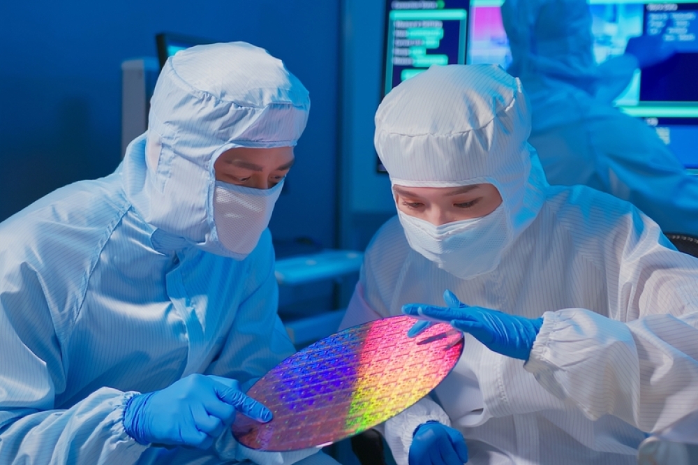
The funding for Purdue will support research to develop innovative materials and designs that will lead to faster, more efficient chips for use in everything from smartphones to AI systems. Semiconductor research is a key pillar of Purdue Computes, a strategic university initiative to further scale Purdue’s research and educational excellence. In addition to leading workforce efforts in the country and landing large-scale industry partnerships, Purdue is proven again and again as the research leader in this foundation of the digital economy.
“These grants will build on and expand the critical semiconductor research that Purdue is known for throughout the world,” said Karen Plaut, executive vice president for research. “Receiving grants from the NSF and major semiconductor corporations in each of the available topic areas underscores Purdue’s reputation as a leader in chips research.”
The new grants support these Purdue projects:
• Bridging Atomic Layers and Foundation Models: An Indium-Oxide-Based Versatile Neural Computing Platform. This work focuses on creating new computing systems using indium oxide, a material that is only a few atomic layers thick. This platform mimics the way human brains process information, which could lead to smarter, faster and more energy-efficient AI systems. The project will be led by Haitong Li, assistant professor of electrical and computer engineering, with Peide Ye, the Richard J. and Mary Jo Schwartz Professor of Electrical and Computer Engineering, and Anand Raghunathan, the Silicon Valley Professor of Electrical and Computer Engineering.
• High-Resolution Imaging of Defects in Semiconductors: Detection, Reliability and Mitigation. This project will use advanced imaging techniques to find and study minute defects in semiconductor materials. Detecting defects at a very detailed level early in the manufacturing process helps improve semiconductor quality, performance and reliability. Leading this study is Nikhilesh Chawla, the Ransburg Professor in Materials Engineering, with Charles Bouman, the Showalter Professor of Electrical and Computer Engineering; Hany Abdel-Khalik, professor of nuclear engineering; and Eshan Ganju, postdoctoral researcher in materials engineering.
• Strain and Temperature Ex-Situ Processing of Ferroelectric Oxides (STEP FOx) for BEOL Performance. This research is aimed at improving the processing methods of ferroelectric oxides. By carefully controlling the temperature and stress on the material during manufacturing, the researchers hope to enhance the material’s performance, which will help create more reliable and efficient electronic devices, especially in the “back-end-of-line” (BEOL) stages, which are key in the production of advanced computer chips. This work is being led by Thomas Beechem, associate professor of mechanical engineering.
Purdue investigators also are participating in a team led by Texas A&M:
• SPRINT: Scalable, High Performance and Reliable Interconnect Technologies Based on Interface Co-Design. This project aims to develop a new way to synthesize copper nanowires and design effective encapsulation layers based on two-dimensional materials. These break the paradigm-limiting current interconnect technology and enable next-generation high-performance and energy-efficient computer chips. Participating are Zhihong Chen, professor of electrical and computer engineering, and Sumeet Gupta, Elmore Associate Professor of Electrical and Computer Engineering.
“The nation’s semiconductor challenge is a Purdue priority,” said Mark Lundstrom, chief semiconductor officer and head of the university’s Semiconductor Task Force. “This funding from NSF and its corporate partners confirms that the work we are doing is critical to the advancement of the U.S. chip industry and all the current and future technological necessities that rely on it.”


