Loading...
News Article

JX Advanced Metals USA opens in Mesa, Arizona

News

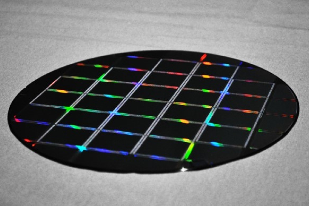
JX Advanced Metals Corporation (has been constructing a new plant in Mesa, Arizona, in order to strengthen its sputtering target business for semiconductors and develop new businesses in the US.

Last week, the group company, JX Advanced Metals USA, celebrated the grand opening of its new state-of-the-art plant with a ribbon-cutting ceremony attended by key company representatives and local dignitaries.

As advanced semiconductor manufacturers build one new base after another, Arizona is becoming a key location for the US semiconductor industry. JXUSA is responsible for manufacturing semiconductor sputtering targets and providing services in close proximity to customers, and the launch of the new plant will further strengthen this role. By introducing advanced equipment, the new plant has automated the process from machining to inspection, which has greatly improved productivity. It has been in trial operation since July this year, with full-scale production set to commence in early 2025.

At the ceremony, Suwabe Takeshi, General Manager of the Thin Film Materials Division, said: "Recent developments in IT, AI, and mobility in the United States are remarkable. We would like to contribute to the development of the industry by supplying cutting-edge semiconductor materials from the new plant." In addition to Suwabe's remarks, the ceremony featured speeches by Mesa Mayor John Giles, Mesa Councilmember Scott Somers, and Devin Patterson, Vice President of Business Development at the Arizona Commerce Authority.

The plant has a site roughly six times larger than the existing site in Chandler, Arizona, and there is still plenty of room for expansion. In the future, it will not only flexibly expand sputtering target production capacity, but also serve as a site for new business development, and the Company intends to make it the center of US business in the advanced materials field.

As a global leader in semiconductor and information and communications materials, the Company will continue to contribute to progress and innovation toward a sustainable society through the development and supply of high-performance, highly functional advanced materials.

Silicon photonics: accelerating growth in the race for high-speed optical interconnects
CCD-in-CMOS technology enables ultra-fast burst mode imaging
2025 6G A look forward
Critical Manufacturing climbs Deloitte’s Technology Fast 50
Semiconductors: The most important thing you probably know the least about
Imec and partners unveil SWIR sensor with lead-free quantum dot photodiodes
Lattice introduces small and mid-range FPGA offerings
SEMI and SMT inspection solutions at NEPCON Japan 2025
Nordic Semiconductor and Kigen demonstrate Remote SIM Provisioning for Massive IoT
Spirent collaborates with Siemens
Quobly forges strategic collaboration with STMicroelectronics
New standards in pressure measurement systems for the semiconductor industry
IBM delivers optics breakthrough
Semiconductor equipment sales to reach $139 Billion in 2026
Marvell introduces 1.6 Tbps LPO Chipset
ACM research strengthens Atomic Layer Deposition portfolio
CEA-Leti demonstrates embedded FeRAM platform compatible with 22nm FD-SOI node
Lattice introduces small and mid-range FPGA offerings
Solace unlocks full potential of event-driven integration
Advantest to showcase latest test solutions at SEMICON Japan 2024
CEA-Leti device integrates light sensing and modulation
Nordic launches Thingy:91 X prototyping platform for cellular IoT and Wi-Fi locationing
Imec achieves seamless InP Chiplet integration on 300mm RF Silicon Interposer
High-precision SMU
Powering India’s energy future
China’s Nvidia probe puts global investors ‘on notice’
POET Technologies appoints new director
Imec demonstrates core building blocks of a scalable, CMOS-fab compatible superconducting digital technology
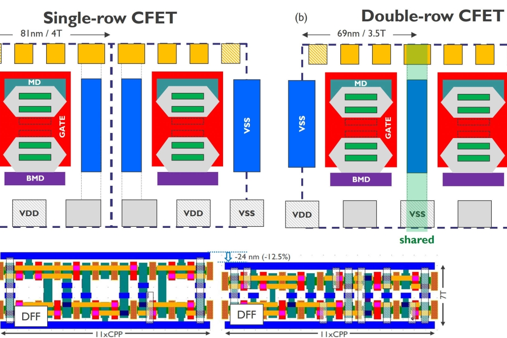
Imec proposes double-row CFET for the A7 technology node
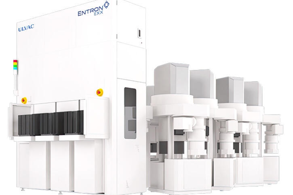
ULVAC launches new deposition system
Beebolt and SEMI Announce Strategic Partnership to Drive Supplier Resilience and Agility
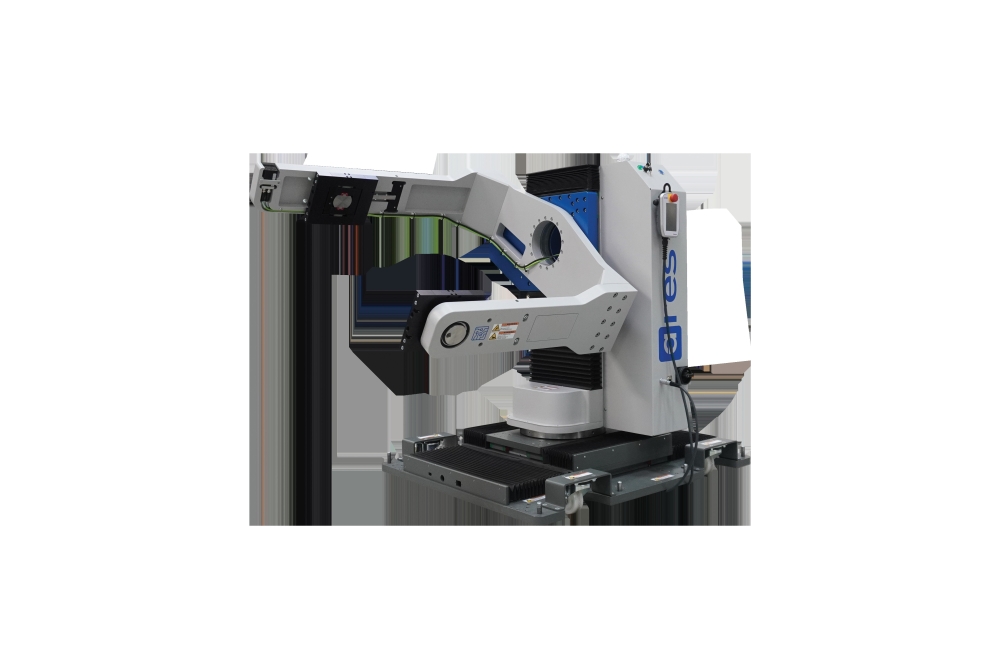
esmo group introduces Automated Final Test Manipulator
×
Search the news archive

To close this popup you can press escape or click the close icon.
Logo
x
Logo
×
Register - Step 1

You may choose to subscribe to the Silicon Semiconductor Magazine, the Silicon Semiconductor Newsletter, or both. You may also request additional information if required, before submitting your application.


Please subscribe me to:


You chose the industry type of "Other"

Please enter the industry that you work in: