The semiconductor industry is set to surpass $1 trillion by 2030, driving industry innovation

Marco Van Der Haar, Market Development Manager Semiconductor at Malvern Panalytical, explains how advanced material analytics is set to transform semiconductor production.
The global semiconductor industry is experiencing an unprecedented surge. In 2025, annual semiconductor sales increased by 25.6% to $791.7 billion, the highest figure on record, and the industry is on track to reach $1 trillion in sales by 2026.*
This explosive growth is fuelled by transformative technologies such as AI, data centres, 5G/6G connectivity, electrified transportation and intelligent edge devices. In this environment, producing large volumes is one thing, but consistently delivering high-quality products at scale is what really sets you apart.
Marco Van Der Haar, Market Development Manager - Semiconductor at Malvern Panalytical, explains how advanced material analytics could make 2026 a pivotal year for the industry.
Material precision: the foundation of next-generation
semiconductors
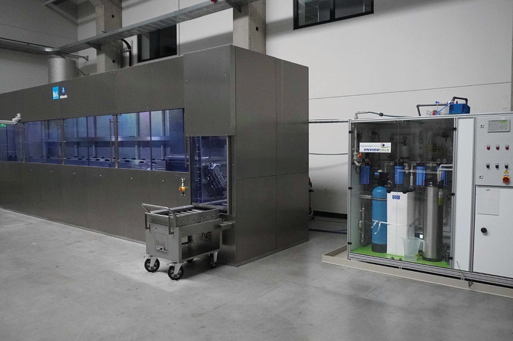
In the upstream part of the semiconductor manufacturing process, precursor materials play a crucial role. They enable deposition processes like chemical vapour deposition (CVD), atomic layer deposition (ALD), and physical vapour deposition (PVD).
Precursor processing often involve powders . These powders
need to meet strict standards as their particle size, shape, surface area, and
chemical compositional affect how thin films form later in the process, hence
impact how well the final devices perform. Even minor errors at this stage can
cause issues later, resulting in lower yields and more waste.

Today, manufacturers use advanced analysis tools to check the size and shape of particles, what their surfaces are like, how porous they are, and what elements they contain. These careful checks help make sure each batch of material acts the same way, so production stays consistent and reliable.
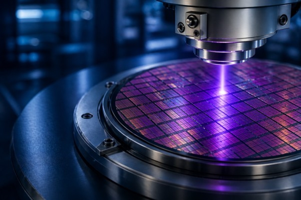
Crystal orientation and thin-film control: precision at
every scale
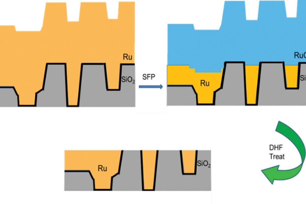
Controlling crystal orientation and lattice integrity of ingots and wafers is essential, especially as new wide-bandgap semiconductors such as SiC, GaN, InP and Ga₂O₃ become more common in high-performance uses. Good lattice alignment helps grinding, cutting, and ion implantation go smoothly and prevents defects that might harm device performance.
Thin-film stacks are increasingly complex, and even atomic-scale variations in for example thickness, density, or composition can impact electrical behavior and long-term reliability. Tools and technologies such as X-ray diffraction (XRD) and X-ray fluorescence (XRF) enable manufacturers to monitor these parameters in real time, maintaining process stability and accelerating development cycles.
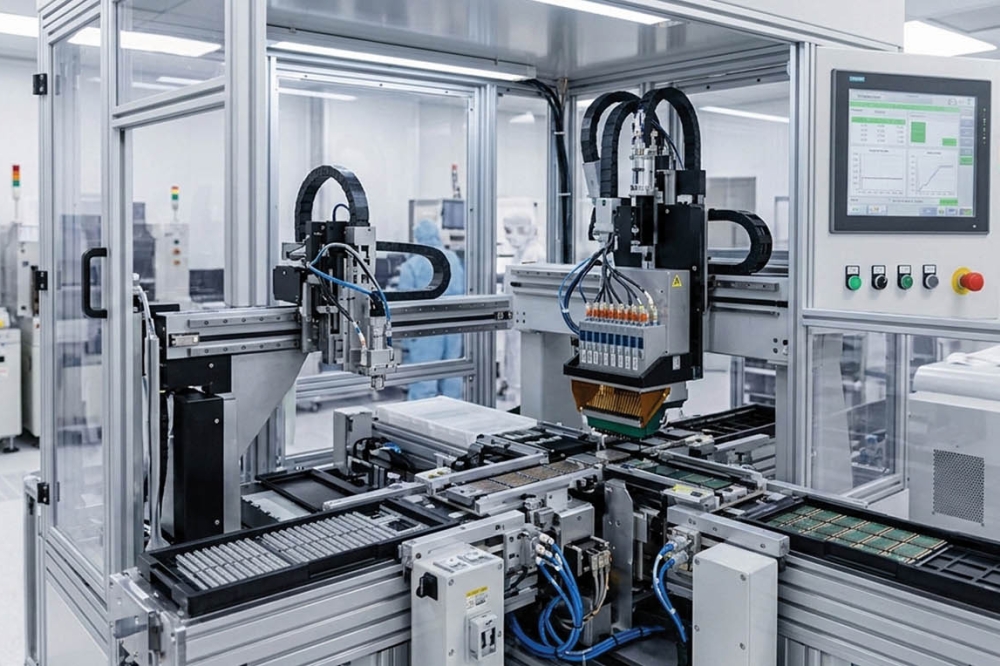
Advanced packaging: from assembly to reliability
As the industry moves toward 2.5D and 3D packaging, chiplets, and high-density interconnects, new material challenges are emerging. Factors like under-bump metallisation uniformity, polymer filler distribution, and epoxy consistency have a direct impact on mechanical strength, thermal management, and how long devices last. By using analytical methods to measure rheology, porosity, and particle distribution of the materials used, manufacturers can keep quality high and continue to innovate in packaging without losing reliability.
Materials analytics: a competitive imperative
The companies that will lead tomorrow are the ones that truly understand their materials, from the first batch of powder to the final packaged product. Using advanced analytics, they can spot problems before they happen, reduce variability, improve yield, and scale with confidence.
By 2026, getting materials right isn’t just a technical challenge; it’s a strategic advantage. Manufacturers who make materials control part of everything they do can deliver next-generation devices with reliability, performance, and trust, setting the pace for the future of the semiconductor industry.
The semiconductor industry is moving into a stage where growth by itself is not enough for success. Control will be what sets leaders apart. As technology advances and production increases and processes get more complex, manufacturers need to better understand how materials behave at every step. If material-level variability goes unnoticed, it can quickly lead to lower yields, reliability problems, and higher costs.
When companies invest in better material insights and strong
process control, they can grow more efficiently and innovate with more
confidence. In the trillion-dollar semiconductor era, precision in materials
leads to precision in devices, and that will be what sets industry leaders
apart.