Chip-processing method could assist cryptography schemes to keep data secure
By enabling two chips to authenticate each other using a shared fingerprint, this technique can improve privacy and energy efficiency.
By Adam Zewe, MIT News Office
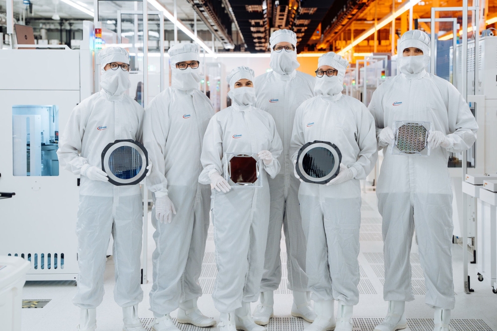
Just like each person has unique fingerprints, every CMOS chip has a distinctive “fingerprint” caused by tiny, random manufacturing variations. Engineers can leverage this unforgeable ID for authentication, to safeguard a device from attackers trying to steal private data.
But these cryptographic schemes typically require secret information about a chip’s fingerprint to be stored on a third-party server. This creates security vulnerabilities and requires additional memory and computation.
To overcome this limitation, MIT engineers developed a
manufacturing method that enables secure, fingerprint-based authentication,
without the need to store secret information outside the chip.

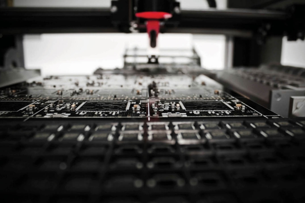
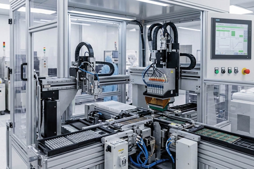
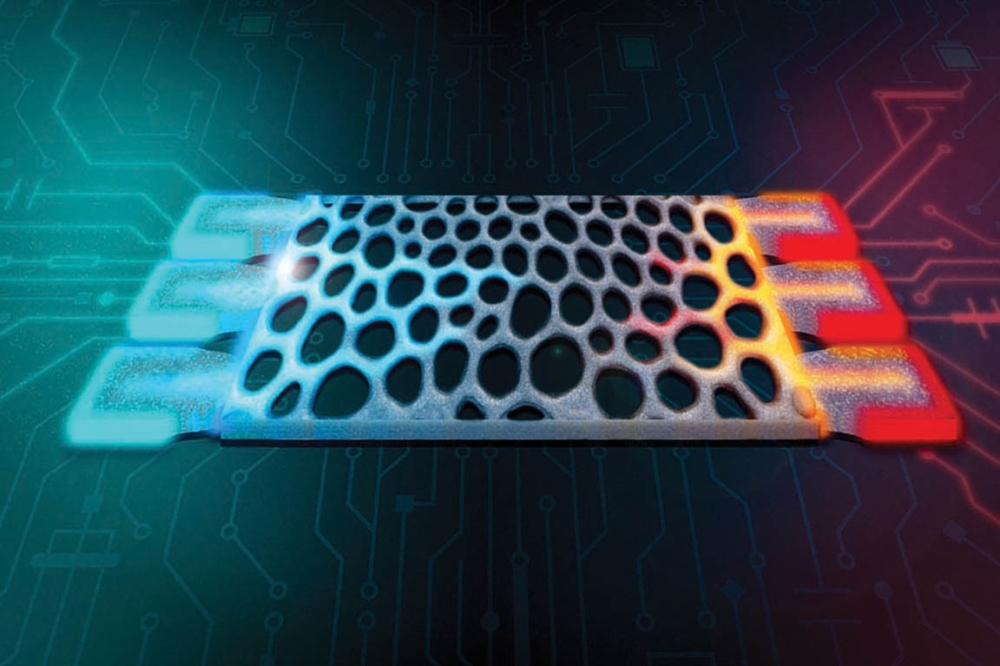
They split a specially designed chip during fabrication in such a way that each half has an identical, shared fingerprint that is unique to these two chips. Each chip can be used to directly authenticate the other. This low-cost fingerprint fabrication method is compatible with standard CMOS foundry processes and requires no special materials.
The technique could be useful in power-constrained electronic systems with non-interchangeable device pairs, like an ingestible sensor pill and its paired wearable patch that monitor gastrointestinal health conditions. Using a shared fingerprint, the pill and patch can authenticate each other without a device in between to mediate.
“The biggest advantage of this security method is that we don’t need to store any information. All the secrets will always remain safe inside the silicon. This can give a higher level of security. As long as you have this digital key, you can always unlock the door,” says Eunseok Lee, an electrical engineering and computer science (EECS) graduate student and lead author of a paper on this security method.
Lee is joined on the paper by EECS graduate students Jaehong Jung and Maitreyi Ashok; as well as co-senior authors Anantha Chandrakasan, MIT provost and the Vannevar Bush Professor of Electrical Engineering and Computer Science, and Ruonan Han, a professor of EECS and a member of the MIT Research Laboratory of Electronics. The research was recently presented at the IEEE International Solid-States Circuits Conference.
“Creation of shared encryption keys in trusted semiconductor foundries could help break the tradeoffs between being more secure and more convenient to use for protection of data transmission,” Han says. “This work, which is digital-based, is still a preliminary trial in this direction; we are exploring how more complex, analog-based secrecy can be duplicated — and only duplicated once.”
Leveraging variations
Even though they are intended to be identical, each CMOS
chip is slightly different due to unavoidable microscopic variations during
fabrication. These randomizations give each chip a unique identifier, known as
a physical unclonable function (PUF), that is nearly impossible to replicate.
A chip’s PUF can be used to provide security just like the human fingerprint identification system on a laptop or door panel.
For authentication, a server sends a request to the device, which responds with a secret key based on its unique physical structure. If the key matches an expected value, the server authenticates the device.
But the PUF authentication data must be registered and stored in a server for access later, creating a potential security vulnerability.
“If we don’t need to store information on these unique randomizations, then the PUF becomes even more secure,” Lee says.
The researchers wanted to accomplish this by developing a
matched PUF pair on two chips. One could authenticate the other directly,
without the need to store PUF data on third-party servers.
As an analogy, consider a sheet of paper torn in half. The torn edges are random and unique, but the pieces have a shared randomness because they fit back together perfectly along the torn edge.
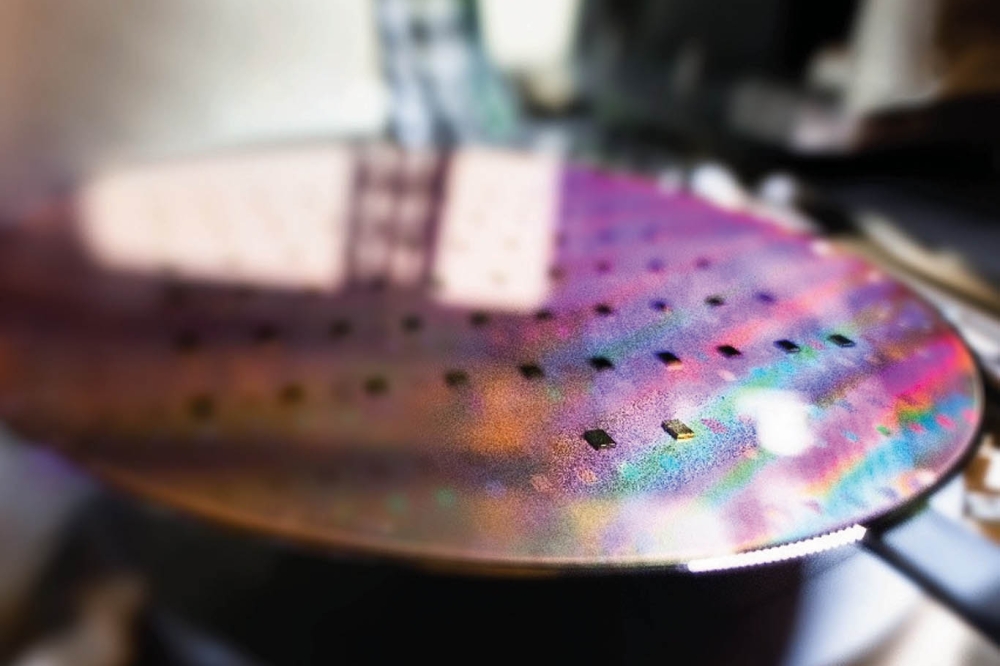
While CMOS chips aren’t torn in half like paper, many are fabricated at once on a silicon wafer which is diced to separate the individual chips.
By incorporating shared randomness at the edge of two chips before they are diced to separate them, the researchers could create a twin PUF that is unique to these two chips.
“We needed to find a way to do this before the chip leaves the foundry, for added security. Once the fabricated chip enters the supply chain, we won’t know what might happen to it,” Lee explains.
haring randomness
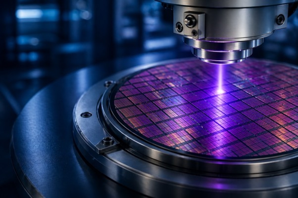
To create the twin PUF, the researchers change the properties of a set of transistors fabricated along the edge of two chips, using a process called gate oxide breakdown.
Essentially, they pump high voltage into a pair of transistors by shining light with a low-cost LED until the first transistor breaks down. Because of tiny manufacturing variations, each transistor has a slightly different breakdown time. The researchers can use this unique breakdown state as the basis for a PUF.
To enable a twin PUF, the MIT researchers fabricate two
pairs of transistors along the edge of two chips before they are diced to
separate them. By connecting the transistors with metal layers, they create
paired structures that have correlated breakdown states. In this way, they
enable a unique PUF to be shared by each pair of transistors.
After shining LED light to create the PUF, they dice the chips between the transistors so there is one pair on each device, giving each separate chip a shared PUF.
“In our case, transistor breakdown has not been modeled well in many of the simulations we had, so there was a lot of uncertainty about how the process would work. Figuring out all the steps, and the order they needed to happen, to generate this shared randomness is the novelty of this work,” Lee says.
After finetuning their PUF generation process, the researchers developed a prototype pair of twin PUF chips in which the randomization was matched with more than 98 percent reliability. This would ensure the generated PUF key matches consistently, enabling secure authentication.
Because they generated this twin PUF using circuit techniques and low-cost LEDs, the process would be easier to implement at scale than other methods that are more complicated or not compatible with standard CMOS fabrication.
“In the current design, shared randomness generated by transistor breakdown is immediately converted into digital data. Future versions could preserve this shared randomness directly within the transistors, strengthening security at the most fundamental physical level of the chip,” Lee says.
“There is a rapidly increasing demand for physical-layer
security for edge devices, such as between medical sensors and devices on
a body, which often operate under strict energy constraints. A twin-paired PUF
approach enables secure communication between nodes without the burden of heavy
protocol overhead, thereby delivering both energy efficiency and strong
security. This initial demonstration paves the way for innovative advancements
in secure hardware design,” Chandrakasan adds.
This work is funded by Lockheed Martin, the MIT School of
Engineering MathWorks Fellowship, and the Korea Foundation for Advanced Studies
Fellowship.
MIT engineers design structures that compute with heat
MIT researchers have designed silicon structures that can perform calculations in an electronic device using excess heat instead of electricity. These tiny structures could someday enable more energy-efficient computation.
In this computing method, input data are encoded as a set of temperatures using the waste heat already present in a device. The flow and distribution of heat through a specially designed material forms the basis of the calculation. Then the output is represented by the power collected at the other end, which is thermostat at a fixed temperature.
The researchers used these structures to perform matrix vector multiplication with more than 99 percent accuracy. Matrix multiplication is the fundamental mathematical technique machine-learning models like LLMs utilize to process information and make predictions.
While the researchers still have to overcome many challenges to scale up this computing method for modern deep-learning models, the technique could be applied to detect heat sources and measure temperature changes in electronics without consuming extra energy. This would also eliminate the need for multiple temperature sensors that take up space on a chip.
“Most of the time, when you are performing computations in an electronic device, heat is the waste product. You often want to get rid of as much heat as you can. But here, we’ve taken the opposite approach by using heat as a form of information itself and showing that computing with heat is possible,” says Caio Silva, an undergraduate student in the Department of Physics and lead author of a paper on the new computing paradigm. Silva is joined on the paper by senior author Giuseppe Romano, a research scientist at MIT’s Institute for Soldier Nanotechnologies and a member of the MIT-IBM Watson AI Lab. The research appears in Physical Review Applied.
Turning up the heat
This work was enabled by a software system the researchers
previously developed that allows them to automatically design a material that
can conduct heat in a specific manner.
Using a technique called inverse design, this system flips the traditional engineering approach on its head. The researchers define the functionality they want first, then the system uses powerful algorithms to iteratively design the best geometry for the task.
They used this system to design complex silicon structures, each roughly the same size as a dust particle, that can perform computations using heat conduction. This is a form of analog computing, in which data are encoded and signals are processed using continuous values, rather than digital bits that are either 0s or 1s.
The researchers feed their software system the specifications of a matrix of numbers that represents a particular calculation. Using a grid, the system designs a set of rectangular silicon structures filled with tiny pores. The system continually adjusts each pixel in the grid until it arrives at the desired mathematical function.
Heat diffuses through the silicon in a way that performs the
matrix multiplication, with the geometry of the structure encoding the
coefficients.
“These structures are far too complicated for us to come up
with just through our own intuition. We need to teach a computer to design them
for us. That is what makes inverse design a very powerful technique,” Romano
says.
But the researchers ran into a problem.
Due to the laws of heat conduction, which impose that heat
goes from hot to cold regions, these structures can only encode positive
coefficients.
They overcame this problem by splitting the target matrix into its positive and negative components and representing them with separately optimized silicon structures that encode positive entries. Subtracting the outputs at a later stage allows them to compute negative matrix values.
They can also tune the thickness of the structures, which allows them to realize a greater variety of matrices. Thicker structures have greater heat conduction.
“Finding the right topology for a given matrix is challenging. We beat this problem by developing an optimization algorithm that ensures the topology being developed is as close as possible to the desired matrix without having any weird parts,” Silva explains.
Microelectronic applications
The researchers used simulations to test the structures on simple matrices with two or three columns. While simple, these small matrices are relevant for important applications, such as fusion sensing and diagnostics in microelectronics.
The structures performed computations with more than 99 percent accuracy in many cases. However, there is still a long way to go before this technique could be used for large-scale applications such as deep learning, since millions of structures would need to be tiled together. As the matrices become more complicated, the structures become less accurate, especially when there is a large distance between the input and output terminals. In addition, the devices have limited bandwidth, which would need to be greatly expanded if they were to be used for deep learning.
But because the structures rely on excess heat, they could be directly applied for tasks like thermal management, as well as heat source or temperature gradient detection in microelectronics.
“This information is critical. Temperature gradients can cause thermal expansion and damage a circuit or even cause an entire device to fail. If we have a localized heat source where we don’t want a heat source, it means we have a problem. We could directly detect such heat sources with these structures, and we can just plug them in without needing any digital components,” Romano says.
Building on this proof-of-concept, the researchers want to design structures that can perform sequential operations, where the output of one structure becomes an input for the next. This is how machine-learning models perform computations. They also plan to develop programmable structures, enabling them to encode different matrices without starting from scratch with a new structure each time.
Reprinted with permission of MIT News.