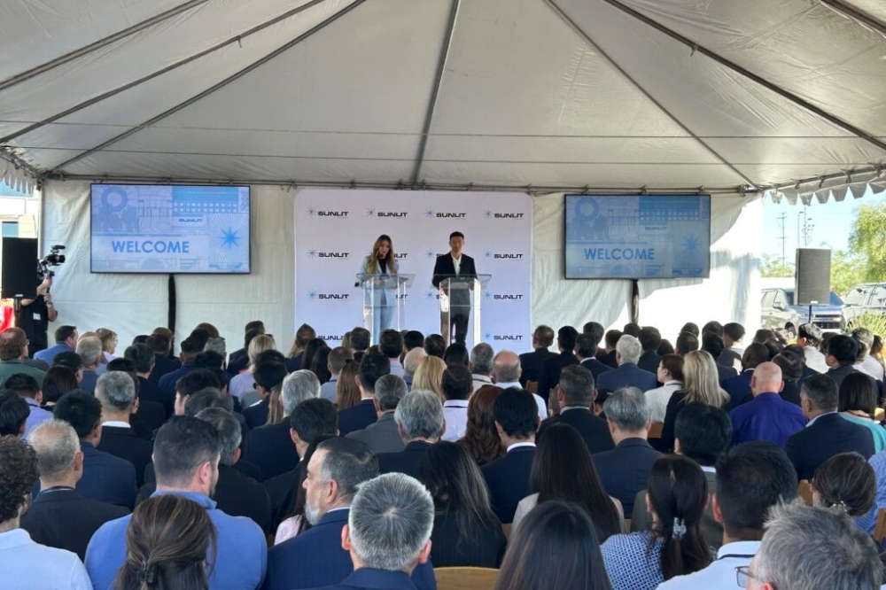
UMC Circular Economy & Recycling Innovation Center breaks ground
The first R&D center for waste recycling in the Southern Taiwan Science Park.
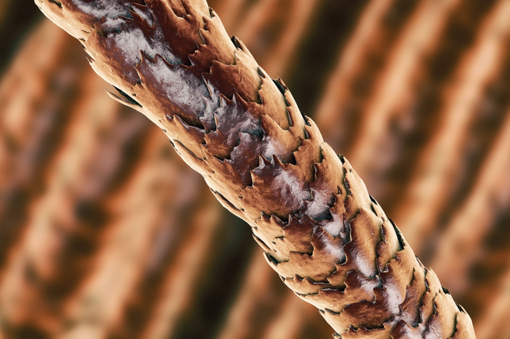
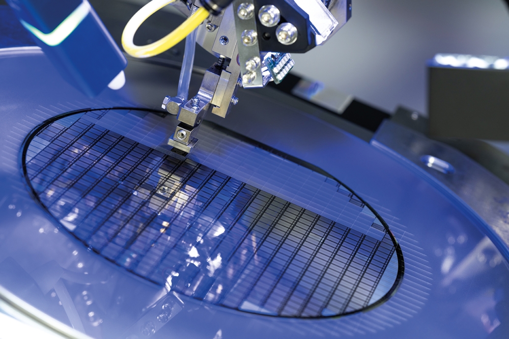
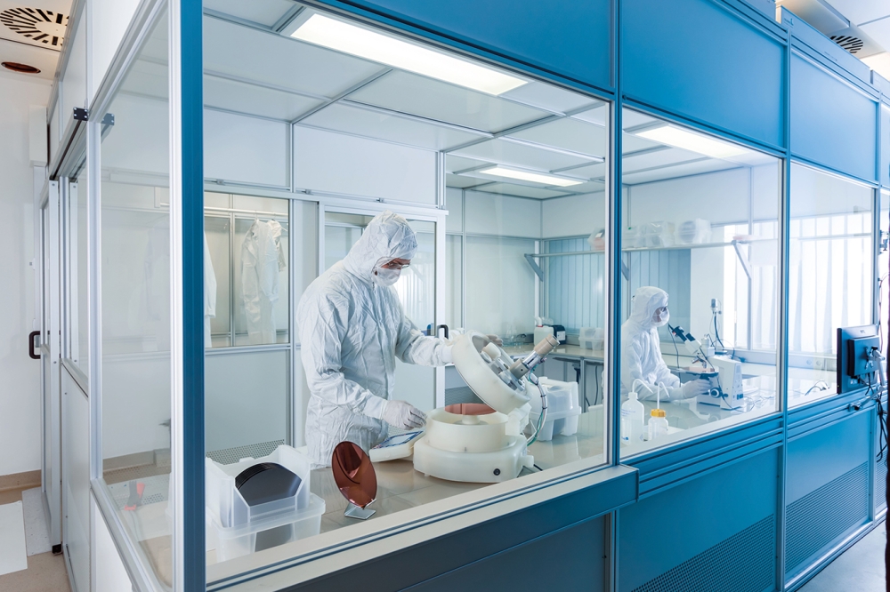
United Microelectronics Corporation recently held a groundbreaking ceremony for its Circular Economy & Recycling Innovation Center, which will be established at its Fab 12A in Tainan, Taiwan. The NT$1.8 billion (US$58.8 million) facility will be the first waste recycling R&D center in the Southern Taiwan Science Park, serving as an important contributor for sustainable circular economy in Taiwan. After the center begins operating in 2025, it is expected to reduce 15,000 metric tons of semiconductor manufacturing waste annually.
"UMC has invested in Taiwan for more than four decades, including in our flagship Fab 12A, the manufacturing and R&D hub for our specialty process technologies. While we have continued to pursue capacity expansions and enhance our R&D capabilities, UMC is also deeply committed to our corporate sustainability goals. The Circular Economy & Recycling Innovation Center will serve as the center of our efforts to maximize resource recovery and minimize waste,” said SC Chien, UMC's Co-President and Chief Sustainability Officer. “Working hand in hand with our value chain partners, we believe we can raise the bar for circularity in Taiwan, and enhance our industry’s competitiveness through sustainable practices.”
In the first phase, UMC's Circular Economy & Recycling Innovation Center will process waste produced during IC manufacturing processes into products that can be reused or sold, such as turning liquid waste and sludge into industrial-grade products. As for waste solvents that cannot be purified, the thermal cracking process will be applied to produce fuel gas to be reused within the facility. In the second phase, the Center will further develop thermal cracking technology that can directly convert waste solvents and plastics into energy supply. Once operational, the facility is expected to reduce waste from UMC’s Taiwan fabs by one-third, and create around NT$100 million worth of value-added products.
UMC has invested in a number of circular economy initiatives over the years, such as decreasing outsourced waste disposal by promoting resource reuse within its fabs. Estimated to lower carbon emissions by around 5,000 tons per year, this program reduces the need for waste transportation and raw material mining, while also mitigating the risks of transporting waste to external facilities. In addition, Fab 12A has introduced an electrolysis process to convert copper sulfate liquid waste into copper tubes with re-sale value, expected to generate more than NT$13 million of revenue per year. Anther initiative in progress is the recycling of used photomasks, which are cleaned on-site to remove patterning and resold as quartz substrates for optical products.
With a total floor area of around 9,000 square meters, the Circular Economy & Recycling Innovation Center is designed in compliance with green building codes, and will also act as an education center to promote circular economy and environmental protection to the young generation. Using this center as a base, UMC will work closely with waste management service providers and raw material suppliers to develop innovative recycling methods and projects, contributing to a better, more sustainable future through collaborations together with value chain partners.