Why new developments in MEMS are fundamental for next-generation devices
Advances in MEMS are set to be crucial for the future of sensors and mobile phones, but there are many other applications.
By Dr. Josep Montanyà i Silvestre, CEO at Nanusens
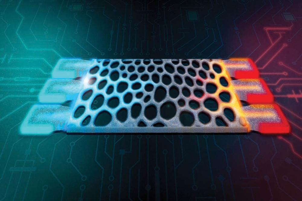
Sensors have tiny mechanical parts that move as a result of a specific stimulus and this movement is identified to form an electrical signal. MEMS (Micro-Electro-Mechanical Systems) technology is fundamental in the design and development of high functioning sensors and capacitors which are needed for next-generation devices.
With traditional MEMS there are some significant barriers, but there have been new developments in MEMS that are designed to address these issues.
Novel MEMS technology looks set to be at the heart of cutting-edge sensors and it is also being leveraged to deliver a solution to the challenge of creating better RF front ends for 6G.
Barriers with traditional MEMS
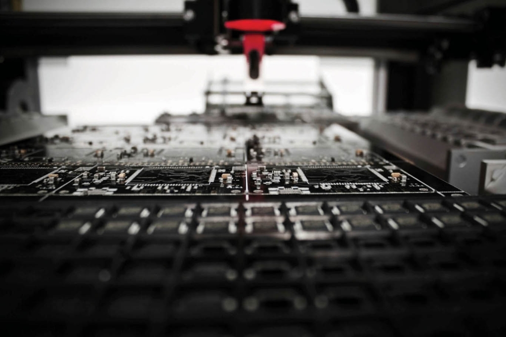
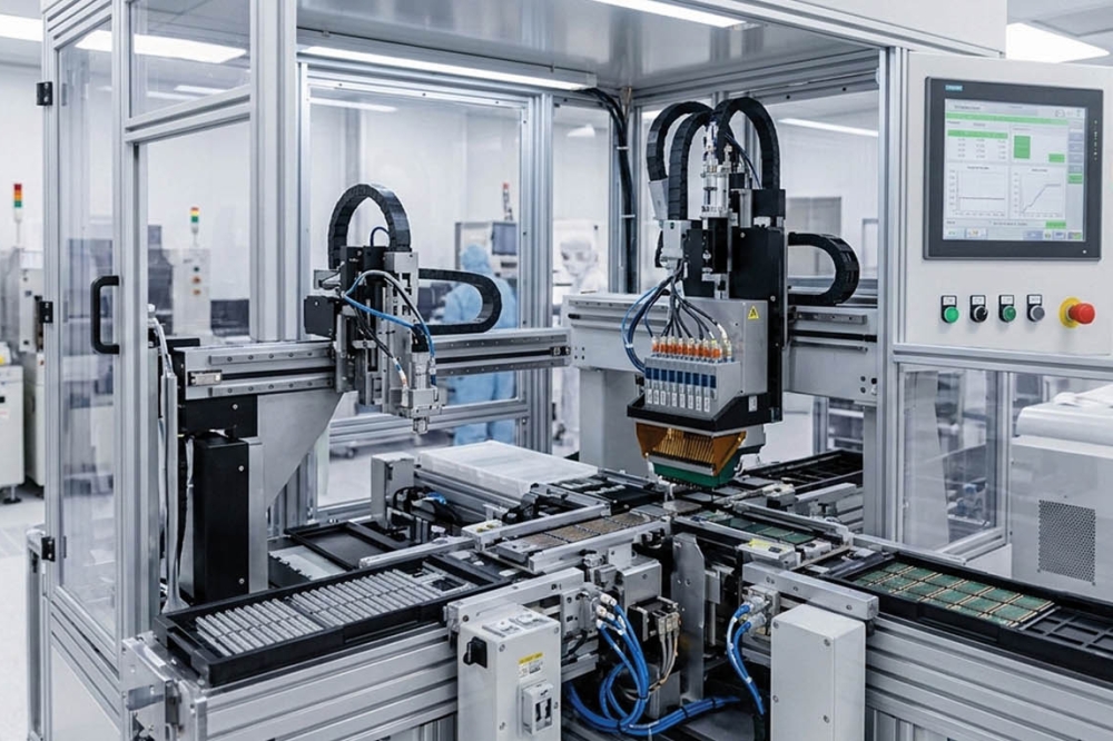
Traditional MEMS involves bespoke design processes that can take years to perfect. MEMS production is usually undertaken on a custom line by specialized companies using proprietary processes to build each MEMS structure. Small variations during MEMS manufacturing can cause performance problems, so yields tend to be relatively low when compared to standard semiconductor manufacturing. Therefore, costs are high, scalability is a challenge and time-to-market is considerable for traditional MEMS devices.
Size is another important issue. Traditional manufacturing
builds a MEMS structure on a tiny sliver of silicon. These are either packaged
into the familiar black unit with wire connections to be mounted on a PCB or
fixed beside the main chip as a bare die.
Both are quite large and expensive, with no options to reduce size or costs. Furthermore, there are sensitivity and noise concerns that mean MEMS devices can be rather fragile and impacted by thermal noise. Power consumption is also a problem for some of these devices.
Modern sensors require small multiple elements to be
embedded in a single package to achieve the enhanced functionality of the
next-generation of smart wearables. Demand for MEMS is accelerating, but in
order to keep up with the growing appetite across the globe for more complex,
compact, power-efficient and robust sensors and devices, fresh developments in
MEMS need to be adopted and the key barriers with traditional MEMS must be
overcome.
New developments in MEMS
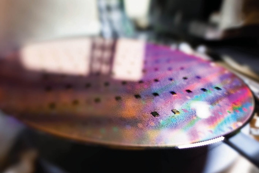
There is a company that has been focused on resolving these issues with MEMS for many years. Nanusens has made a major breakthrough with a novel technology approach, creating MEMS structures using the metal layers within a CMOS (Complementary Metal-Oxide Semiconductor) chip. This means that specialized processes are no longer needed and the costs are significantly lower due to the huge economies of scale achieved when manufacturing in giant CMOS fabs.
In terms of size, there has also been a big change. Traditional MEMS structures have feature sizes of one micron or larger. However, as the Nanusens process occurs within the CMOS chip the structures are nanoscopic in size rather than microscopic. These NEMS (Nano Electro Mechanical Systems) structures have features of 0.3 microns or less - a 100x area reduction.
A traditional MEMS sensor package has two chips, one with the MEMS structure built on it and a second with the control electronics. The package size is around 2.6mm3. In contrast, a Nanusens NEMS sensor package has it all on one chip and the size is only 0.6mm3. As a result, there is room for multiple sensors to be embedded into the chip and power requirements are much lower.
Enhanced performance is another advantage with this novel
NEMS due to very small parasitic capacitances. With traditional MEMS, where the
structure is placed on top of a CMOS wafer or wire bonding is involved, there
is a parasitic capacitance of around a picofarad.
The MEMS-in-CMOS approach offers a rather considerable signal to noise ratio improvement as this falls to around ten femtofarads or less.
A new way to measure the capacitance of the Nanusens nanosensors has also been developed using a digital circuit instead of the traditional analog method. Consequently, in order to cut power consumption and size even further, the sensor designs and digital circuit can be ported to smaller nodes without any reliability concerns.
Technology overview
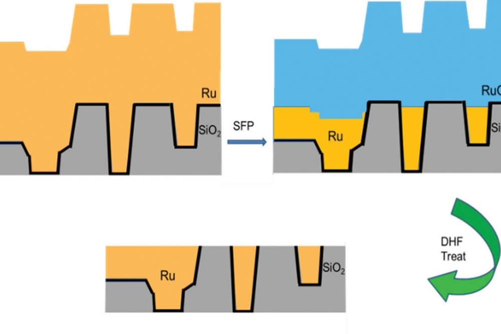
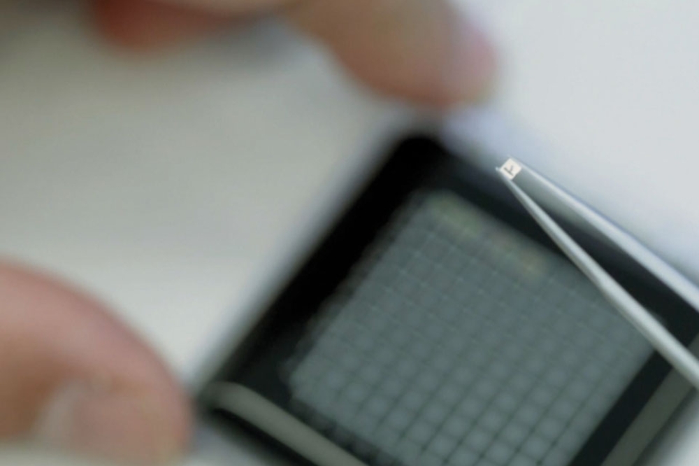
The Nanusens nano-mechanical devices are created using the metal layers in the back-end of the CMOS wafer. Some of the silicon oxide that is surrounding the layers has to be etched away, so that these can move. To do this Hydrofluoric Acid is applied to the wafer during the vapor stage (vHF) using standard equipment. The vHF etches away the silicon oxide around the metal layers through the pad opening placed above the MEMS cavity. This maskless, simple and swift process typically only takes 30 minutes and occurs after the CMOS process is completed.
Although the new approach may not seem overly complicated, it has certainly been a challenge to make this work effectively. Until now metal layers have never been used in a CMOS process to create mechanical devices as their mechanical properties are not well suited for this. In contrast to a custom MEMS process, these are thin, with large residual stress. Even more concerning, there is a large vertical stress gradient. However, with this new process comes some significant advantages, such as; submicron feature sizes and gaps, and a minimal capacitance to connect the MEMS and the ASIC, as well as a large number of structural layers that allow for creative 3D solutions.
Technology use case – improving sensor data processing
Rather than just sending sensor data to the AI processing center, there is now another idea being considered, processing sensor data locally before sending it to the Cloud. There is good reason for this approach. There are some situations when sensors are capturing data where there is nothing for most of the time. For example, a smart microphone where there is often silence. Sending silence to the Cloud is simply wasting communication bandwidth and computing power in the Cloud. It would be much better to process this sensor data locally where the smart microphone is located. Then this will be sent to the Cloud for processing at the AI center when a person is talking or some sound needs to be analyzed.
Edge processors are digital or AI processors that are optimized to have low power consumption and are located with each other with the sensors. When sensors and edge processors are placed together the term AIoT (Artificial Intelligence of Things) is used. Nanusens can build the edge processor monolithically with the sensors into the same CMOS die, which shrinks the size and cuts power consumption. Another justification for local sensor data processing is with health monitoring devices. The processed results can be sent to the Cloud without including all the patient’s details, so that the privacy of the user can be protected.
Technology use case – finding a solution for 6G RF front end
The mobile phone industry has seen many exciting developments over the last 30 years. Innovation in this sector looks set to continue as smart mobile devices have become a critical part of most people’s daily lives. There is a big buzz around the arrival of 6G, but technology bottlenecks exist that must be addressed before adoption of 6G can really take off. For example, 6G mobile phones will need to operate at a wide range of frequency bands and often at higher frequencies.
Therefore, the antenna tuning circuit found at the RF front end will have to be totally rebuilt. Currently, 5G phones use a set of distinct capacitors on a PCB. These are connected and disconnected to the antenna in real time by a separate control chip created by leveraging Silicon-On-Insulator (SOI) technology.
However, this method results in ohmic losses at higher frequencies, with the antenna efficiency falling below an acceptable level. Operating at high frequencies with high voltages would also distort the signal and 6G demands very high linearity.
With the Nanusens approach, building MEMS structures using standard CMOS can be implemented to create digitally tunable MEMS capacitors with the CMOS layers. This provides the low losses and high linearity that is required for 6G phones. These RF Digitally Tunable Capacitors (DTCs) offer a solution that meets the needs of the RF front end of 6G mobile phones.
The nanoscale capacitors are embedded into the same chip as the control circuitry to deliver a far smaller, single chip solution than the SOI approach, and with far greater levels of performance, power-efficiency and reliability. Following tests on these capacitors for 5G the results demonstrate that there is a 90% increase in talk times. For 6G, the power-efficiency at the antenna can be enhanced even more with this technology. With production taking place in giant CMOS fabs in great volumes this means that it will be possible to satisfy the huge demand for use in 6G phones.
Potential applications
Advances in MEMS are set to be crucial for the future of
sensors and mobile phones, but there are many other applications. Nanusens is
developing this innovative MEMS technology for the next generation of embedded
sensors such as gyroscopes, magnetometers, pressure sensors, IR imagers and gas
sensors as variants on the accelerometer design. The opportunities for MEMS are
vast.