Revolutionising Silicon MEMS Technology With CMOS
InvenSense, a pioneer in MEMs technology says it is using a new game-changing strategy.
The company is offering its proprietary MEMS fabrication process for use by all MEMS developers on a limited licensing basis.
One of the processes known as NF-Shuttle, enables emerging MEMS developers to focus on innovation rather than time consuming and costly specialised fabrication development.
"At InvenSense, we are committed to seeing the proliferation of MEMS products on our proprietary fabrication platform not only in inertial sensors but also in resonators, microphones, switches, pressure sensors, RF tuners, etc.," points out Steve Nasiri founder and CEO of InvenSense.
"We have found there are many companies and universities that have brilliant ideas yet they need to spend as much as 60 to 80 percent of their time and development resources on MEMS-related fabrication due to lack of any viable off-the-shelf processes. With our platform it is now possible to bring innovative MEMS products to market much faster and at significantly lower costs."
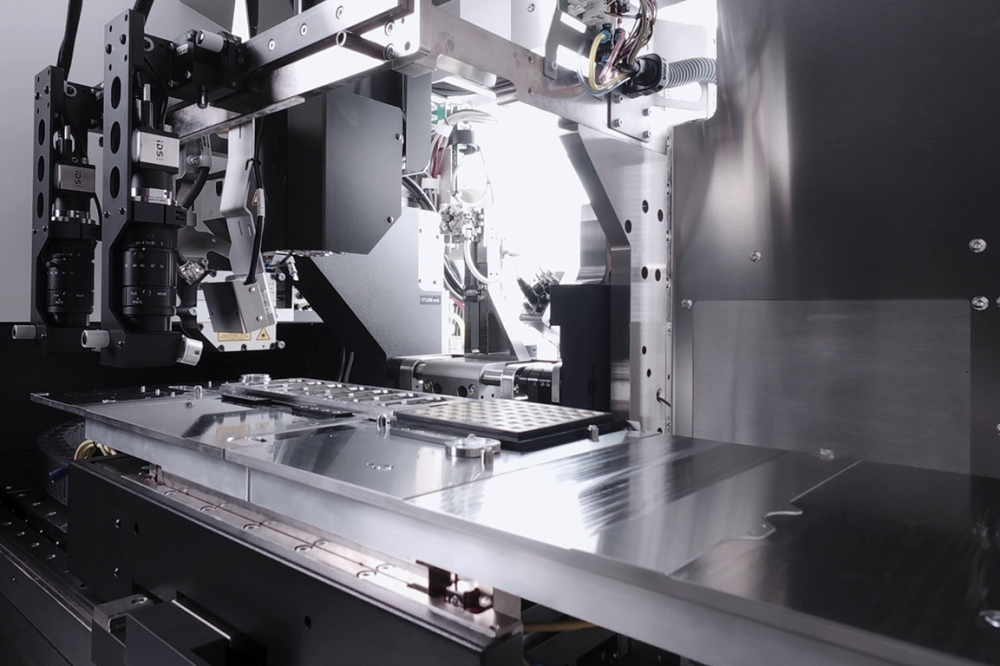
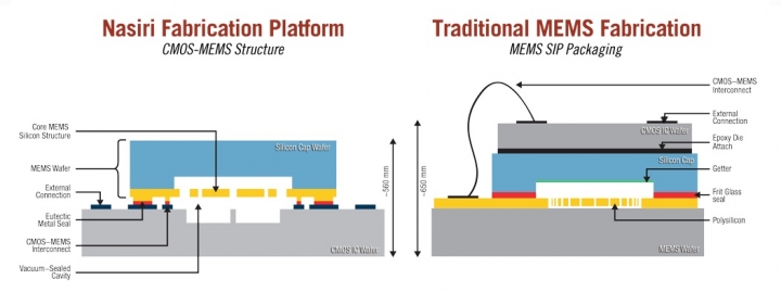
The InvenSense NF-Shuttle is a silicon CMOS-MEMS platform where mask costs are split amongst multiple users as they can purchase "seats" on the same mask. The company says this approach reduces production costs for participants to a fraction of the total and thus provides a greater opportunity to verify their advanced designs and prototypes in silicon.
The initial shuttle test run which took place in January was offered to selected participants from University of California Berkeley with U.C Davis, Stanford University, and a few other institutions.
The short turn-around time, cost and results, observed by the aforementioned institutions have secured space on InvenSense's next two shuttles. InvenSense's second shuttle is scheduled for May 30th, with an increased number of selected participants. The company is opening a third shuttle to a broader audience and is taking orders now. The third shuttle is expected for takeoff on December 5, 2012.
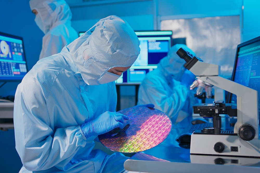
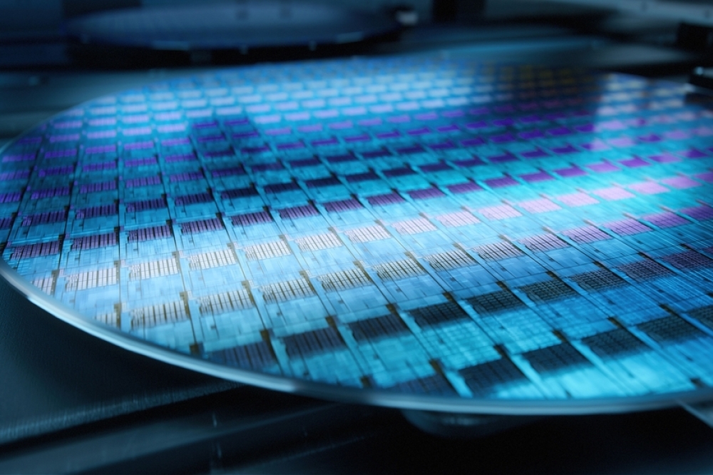
The InvenSense NF Platform has been used to produce over 200 million MEMS units to date. The disruptive, patented Platform is able to combine MEMS on CMOS (or CMOS-MEMS) in a small, cost effective standard package resulting in significant performance, reliability, integration and cost benefits.
Combining a MEMS wafer with an industry standard CMOS wafer allows InvenSense to reduce the number of MEMS manufacturing steps, perform wafer-level testing, and use chip-scale packaging. This reduces back-end costs of packaging and testing and improves overall yield.