3D-Micromac accelerates roll-to-roll laser micromachining with microFLEX
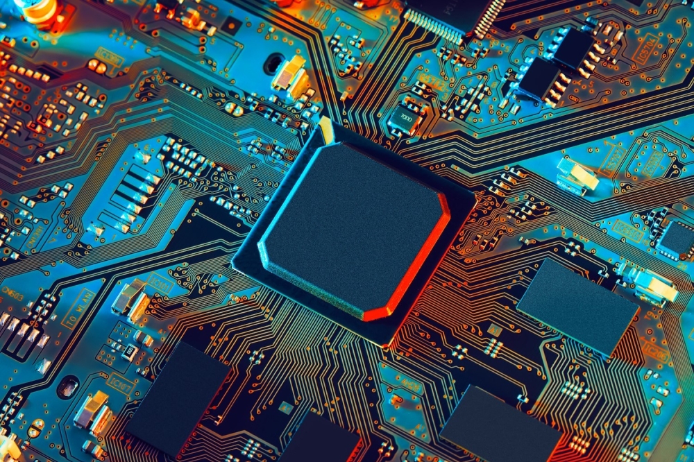
Lasers are versatile industrial tools that today are mainstays within
many semiconductor and photovoltaic manufacturing processes. The
accuracy, repeatability, speed and cost-effectiveness of laser
micromachining was largely absent from roll-to-roll (R2R) thin-film
manufacturing until 3D-Micromac brought its innovative microFLEX system
from the lab to fabs across the globe.
By Mark Andrews, TECHNICAL EDITOR, SILICON SEMICONDUCTOR
Advanced technologies often share a common heritage. The development of drones and quadcopters for example would likely not have occurred when it did were it not for the miniaturized gyroscopes, accelerometers, and microphones first developed for smartphones.
One technology frequently gives rise to another, so in a sense it is not surprising that the roll-to-roll (R2R) technology first developed for web printing was foundational to thin-film manufacturing utilizing a wide range of flexible substrate materials. Thanks to this genesis, products built utilizing flexible electronics and batteries are now enabling wearable medical diagnostic tools, fitness trackers and photovoltaic (PV) cells to name but a few of the most widely recognized applications.
According to Christian Scholz, 3D-Micromac Team Leader for R2R Processing, initial work on the system that would evolve into microFLEX began as a project with the Technical University of Chemnitz (Germany.) An early goal was incorporating a laser module into a R2R printing system. While those first systems brought high accuracy and repeatability to printing, achieving the next step – R2R manufacturing using flexible substrates and laser micromachining – was still years away.
“The Technical University of Chemnitz is very strong in printing technology and they were venturing into printed functionalities – printing simple circuits and things like that in the early 2000s. And they quickly realized that with standard printing technology, you cannot achieve such small feature sizes as would be needed for a printed circuit,” Scholz noted. “Standard graphic printing doesn’t need an accuracy in the range of a few microns since the human eye cannot see those very fine details. But if you want to print electronics, especially if you have multiple layers, then you need to precisely align your first printing step to the next one and the next. Also, the laser has to be very precise to machine at the very right position.”

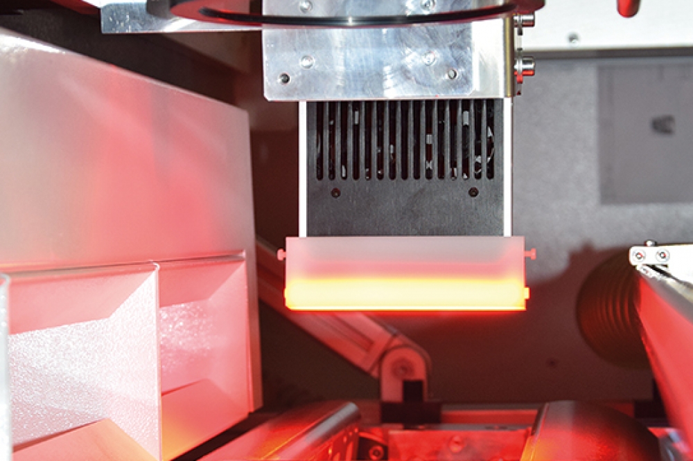
As laser processing is forceless and contactless, microFLEX guarantees a very selective machining of material stacks and extremely thin layers
The potential of manufacturing flexible device components at high speed with extreme precision was tantalizing even as researchers quickly realized that toolsets optimized for paper printing were not accurate enough for manufacturing at micrometer scale. Once 3D-Micromac successfully created a laser micromachining module for print, could the technology be adapted, optimized and transferred to thin-film R2R manufacturing? The answer ultimately proved to be ‘yes,’ but as is often seen in developmental work, adapting technologies frequently involves creating new approaches and machines to work with very different materials, especially at high speeds while retaining micrometer accuracy. 3D-Micromac achieved its goal by creating microFLEX: a cost-effective, reconfigurable laser micromachining system that supports myriad R2R applications for a global customer base.

The modular machine concept of microFLEX allows the system design to be easily adapted to customers’ requests
Today’s R2R machining refers to a family of manufacturing technologies and processes that involve the continuous processing of a flexible substrate that is moving between two moving rolls of rotating material. The speed at which the films are processed depends in part on the width of the material, its thickness, and the processes involved, such as ablation, structuring of flexible solar cells, and so forth.
Advancements in the R2R field have made it an important class of substrate-based manufacturing processes in which subtractive and additive techniques are used to build structures in a consistent manner. High degrees of accuracy are possible, with 3D-Micromac systems often achieving precision within single-digit micron ranges.

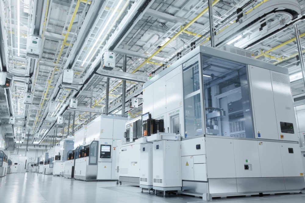
3D-Micromac offers R2R process development and contract manufacturing services for its customers
R2R processes comprise many techniques that, when brought together, help produce rolls of finished material in a highly efficient and economical manner. Chief benefits amongst many are high speed, high volume production. Comparatively low cost and high throughput are the key differentiators of R2R manufacturing compared to conventional techniques such as batch processing, which involves more steps. In comparing different approaches to the manufacture of solar cells, a thin-film R2R process producing CIGS PV cells is four times faster than other techniques, according to the US National Energy Research Laboratory (NERL).

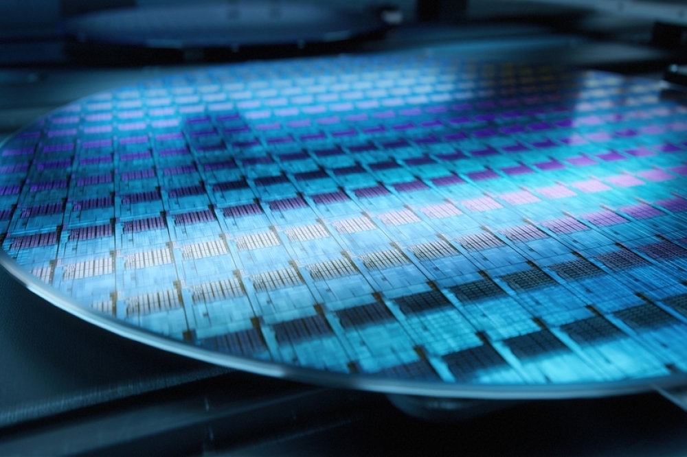
The processing of flexible thin-film photovoltaics has high process stability, reproducibility, and throughput requirements