Achieving ALD consistency is key to maximizing chip yields
Atomic Level Deposition (ALD) has emerged as an increasingly
important aspect of advanced semiconductor manufacturing. The experts at
Swagelok explain the role that valves play in maximizing chip yields.
By Masroor Malik, Market Manager for Semiconductor, Swagelok Company
Moore’s Law, attributed to Fairchild Semiconductor and Intel co-founder Gordon Moore, predicted that chip complexity (density) would roughly double every year, reducing the cost of computing by half. While the original 12-month timeframe has been extended and modified over the years as chip complexity grew, Moore’s prediction in 1965 has largely held true, and the semiconductor industry has worked hard to make it happen.
Maximizing throughput in the increasingly complex and sensitive processes required to manufacture modern microchips is one of today’s biggest challenges for semiconductor producers. Tighter process controls and narrower performance tolerances in production processes represent some primary strategies fabs are using to achieve ever-shrinking device feature size while optimizing chip yields.
As the desire to increase transistor density drove chip architecture innovation, process tool manufacturers have created increasingly complex front-end processes to support design goals and maintain quality, performance and serviceable lifetimes. While today’s definition of ‘advanced node’ has breached 5 nm on the way to 3nm and below, manufacturers can in a sense be divided by how they achieve greater transistor density and/or performance goals while maintaining high, profitable yields. The largest fab operators are increasingly relying on extreme ultraviolet (EUV) lithography to achieve this aim. But the $125 million price for a single EUV lithographic station is evidence that the growing expense of traditional CMOS scaling has led some manufacturers to pursue other paths. Nontraditional innovation includes the move to 2D and 3D structures, wafer bonding, advanced packaging technologies like FOWLP that increases inputs/outputs (I/O), as well as moves to make production processes once seen as novelties fully suitable for high volume manufacturing.
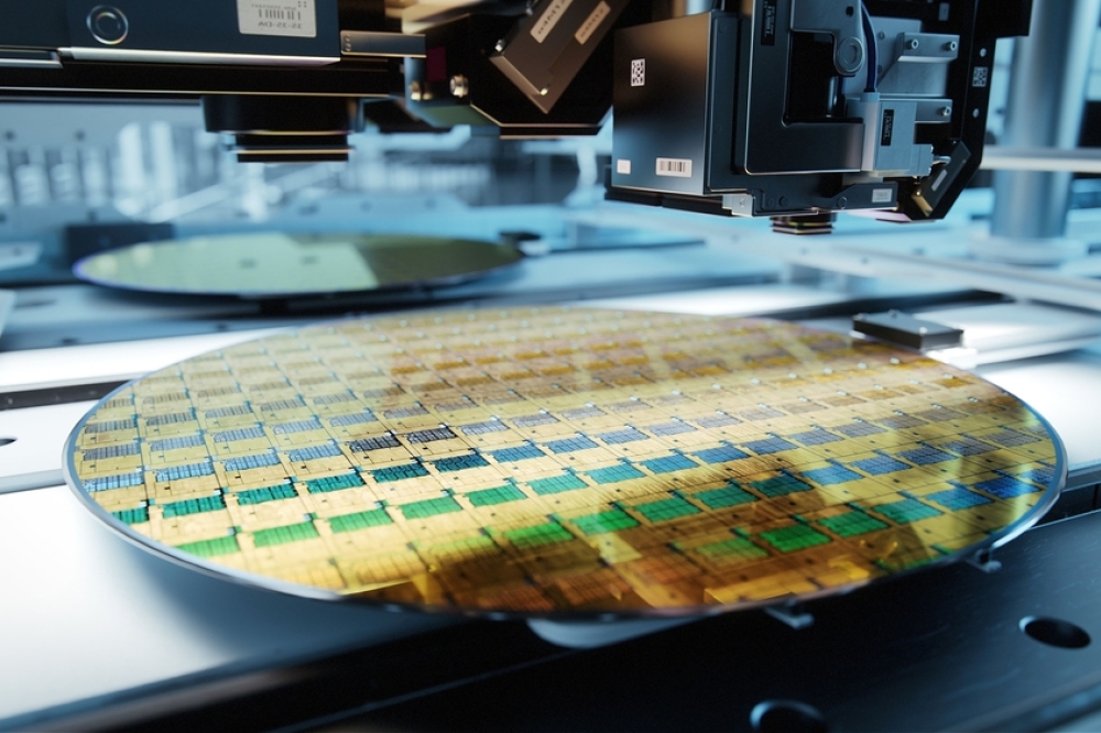
One increasingly popular process used in manufacturing advanced semiconductors is atomic level deposition (ALD). The modern ALD process has become a focal point for achieving increased accuracy and consistency. It has become increasingly evident that high levels of precision in chemical dosing and delivery are essential parts of an optimally productive ALD process. Importantly, that precision must be maintained consistently at every dose. But pulling off both conditions simultaneously becomes inherently more challenging as chip size is reduced. (See Figure 1).
How can fabs achieve such consistency and precision in the ALD process? It has been shown that advanced, well-designed ALD valve technology can contribute to achieving these goals.

Corrosion that forms in the valves, tubing, or fittings, can
produce particles that contaminate the wafer. In ALD, particularly with
liquid or solid precursors, condensation on cold spots or parasitic
deposition in the valves or delivery system can also produce particle
defects and negatively impact yield. Image © 2021 Swagelok Company
At the Intersection of Precision and Reliability
Within the ALD process, semiconductor fabricators are generally working to maintain atomic layer precision in deposited films over an entire 300-millimeter diameter wafer. To give a sense of scale, that is the equivalent of applying a 1-centimeter layer over the entire moon. And in modern semiconductor devices, even the smallest variations in that film (even a few extra atoms) can noticeably and negatively impact end-user device performance.
One significant factor that influences the deposited layers is the specific concentration of chemicals in each atomic layer process dose. Maintaining the proper concentration requires high levels of precision in chemical delivery throughout each dose, necessitating specialized ALD valves to start and stop the flow of chemical reagents into the process chamber in the desired manner. Considering that ALD processes typically involve hundreds of dosing steps, these process valves are actuated continuously. It is not uncommon for valves of this nature to cycle upward of 1 million times each week.
Thus, extremely high-cycle reliability is a requirement. Simultaneously, because process valves may also function as a flow-limiting element in some applications, flow capacity and consistency may also be important to maintain over the life of the valve. In addition, flow consistency from valve to valve will be critical in achieving process matching and in maintaining process consistency after valves have been changed.
Heightened Actuation Speed Contributes to Consistency and Efficiency
Raw actuation speed can also contribute to more efficient production. Faster actuation can compress the time between process steps, and when taken cumulatively, such compression can contribute to a significant reduction in the total processing time.
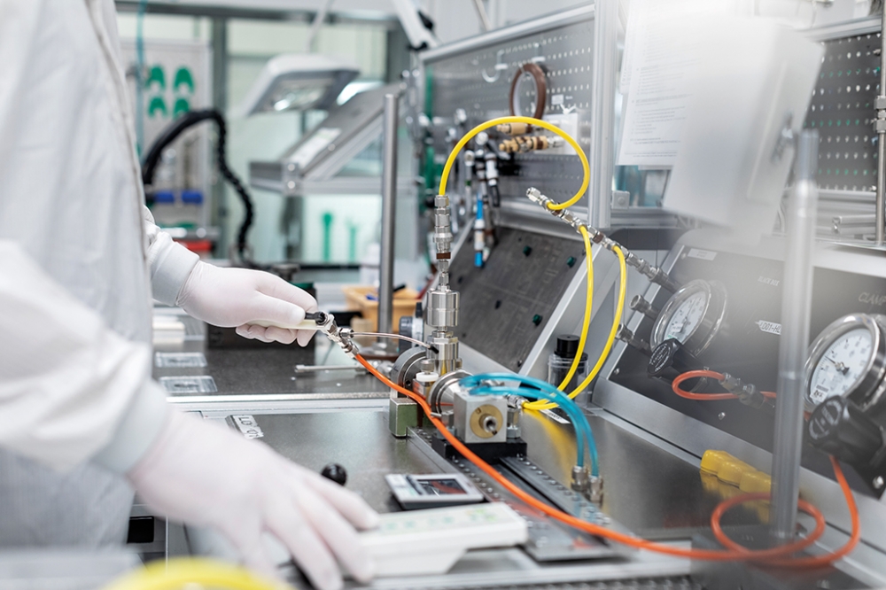
However, it is also important to remember that valves with high, consistent flow and fast, repeatable actuation are only useful if they are compatible with the chemicals being delivered and the temperatures of the delivery system. Corrosion in the valves, tubing, or fittings can produce particles that contaminate the wafer. In ALD, particularly with liquid or solid precursors, condensation on cold spots or parasitic deposition in the valves or delivery system can also produce particle defects and negatively impact yield (See Figure 2).
ALD repeatability is unambiguously linked to the consistency and accuracy of the discrete chemical doses used. Anything that may lead to some form of change or difference within the chemical doses will cause a change or difference in the associated process.
Achieving More Profitable Production
Given the complexity involved in achieving consistent, accurate dosing, there is no single solution to account for all factors that go into devising absolutely consistent and reliable ALD processes. However, there are dependable ways to improve processes that you can take advantage of today.
Advanced ALD process valve technology has evolved to meet the cutting-edge needs of semiconductor chip fabricators and tool OEMs (See Figure 3). Available ALD valves can deliver improved speed, accuracy, and consistency, helping to shorten pulse times while delivering outstanding consistency over many millions of cycles. They also have the potential to help you gain a competitive edge when using such valves in the right application. High-performance, ultrahigh-purity ALD valve technology that features several critical performance characteristics can help tool manufacturers and fabricators optimize processes.
Additionally, working with a knowledgeable team that understands the challenges inherent to atomic layer processes and has experience solving them with high-quality components and service can go a long way toward enhanced accuracy and consistency in your ALD processes.
 Advanced ALD process valve technology has evolved to meet the needs of semiconductor chip fabricators and tool OEMs. Available ALD valves have the capability to deliver improved speed and consistency, helping to shorten pulse times while delivering outstanding consistency over many millions of cycles. Image © 2021 Swagelok Company