Loading...
Interview

Magazine Feature
This article was originally featured in the edition:
2022 Issue 5

Cutting FOPLP pattern distortion

News

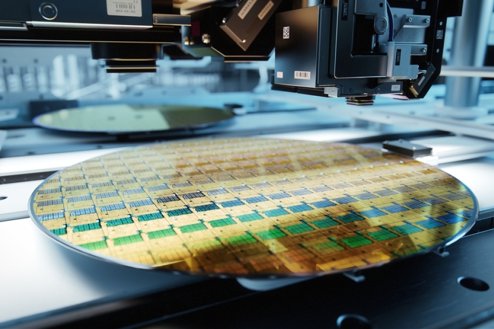
Heterogeneous integration enables multiple chips from varying Silicon processes to deliver superior performance. In large panel packages, present day limits on exposure field size forces manufacturers to ‘stitch’ together multiple reticles, which slows throughput and increases costs. Onto Innovation’s new JetStep® X500 system dramatically increases the exposure field up to 250 x 250 mm, slashing the number of exposures needed and cutting costs in FOPLP applications.

By John Chang, Corey Shay, James Webb and Timothy Chang, Onto Innovation Inc.

Making sure that AI and High Bandwidth Memory stack up
TSMC invest $100 billion in U.S.
Attopsemi expands its I-fuse OTP portfolio on X-FAB’s 180nm Platform
sureCore collaborates with KU Leuven
Myriota and Nordic Semiconductor partner
Premier electronics packaging conference celebrates 75 years of serving the industry
Analog Devices wins up to $105 million in Federal CHIPS funding
GlobalFoundries and MIT collaborate
Stantec to provide design services for €3.2 billion semiconductor assembly and test facility in Italy
Synopsys teams up with SEMI Foundation
Synopsys expands Hardware-Assisted Verification Portfolio
techUK urges the UK Government to speed up the implementation of the National Semiconductor Strategy
Improved gaming, connectivity and AI performance
Aeluma appoints former NVIDIA finance leader Mike Byron to Board of Directors
Imec demonstrates electrical yield for 20nm pitch metal lines obtained with High NA EUV single patterning
Svein-Egil Nielsen joins Nanopower as chair of the board
Salience Labs closes Series A Round
Automated electronics disassembly
MESI 4.0 Summit 2025: Global manufacturers reunite to accelerate digital transformation
Thalia introduces latest version of AMALIA
VyperCore launches VyperLab
NXP to acquire edge AI pioneer Kinara
DeepSeek-R1 1.5B on SiMa.ai for less than 10 watts
Arteris releases the latest generation of Magillem Registers
Baya Systems and Semidynamics collaborate
ams OSRAM receives EU Commission approval for investment grant
Q.ANT and IMS CHIPS launch production of high-performance AI chips
SEMICON Southeast Asia 2025 celebrates 30 years of innovation through collaboration
EMEA Big Data Analytics to hit $5,756.5 million by 2027
3D Semiconductor Packaging market to reach US$ 43.6 billion by 2034
Pfeiffer Vacuum+Fab Solutions achieves validation of emission reduction targets by the SBTi
Infineon introduces CoolGaN G3 Transistor
×
Search the news archive

To close this popup you can press escape or click the close icon.
Logo
x
Logo
×
Register - Step 1

You may choose to subscribe to the Silicon Semiconductor Magazine, the Silicon Semiconductor Newsletter, or both. You may also request additional information if required, before submitting your application.


Please subscribe me to:


You chose the industry type of "Other"

Please enter the industry that you work in:
 
X
Adblocker Detected
Please consider unblocking adverts on this website