Virtual fab focuses on real carbon footprint reductions
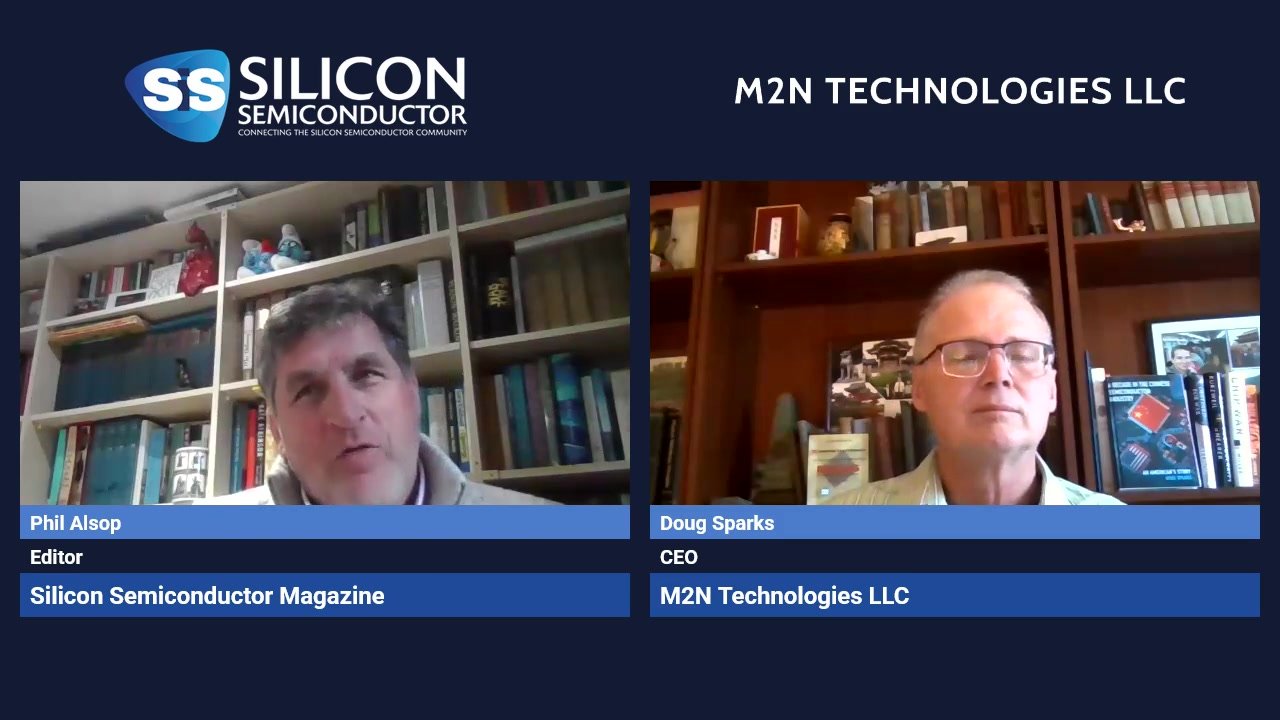
EMILY GALLAGHER, A PRINCIPAL MEMBER OF THE TECHNICAL STAFF AT IMEC,
discusses with Philip Alsop, SiS Editor, the sustainability challenge
facing the semiconductor industry and explains how imec’s recently
launched Virtual Fab is playing an important role in helping to improve
both the understanding and development of environmentally friendly,
patterning-related process solutions.
PA: CO2 emissions associated with integrated circuit manufacturing, I think they’re expected to quadruple over the next decade. Why is that? Simply because of the massive explosion in digital infrastructure, an explosion that is not sustainable?
EG: There are two factors to that quadrupling number. It’s really sort of doubling twice. One time, because of complexity, so going to more advanced nodes, having more process steps involved, that creates a growth. And then the other thing that creates a growth is the volume, so the market itself is getting larger. So those two things together add to the quadrupling. And I agree it’s not sustainable.
There are some low hanging fruit things we can do. One of them is move to greener energy and another one is improved abatement. Those are in the works, planned, but even with those two, we still are about two and a half x off where we need to be to meet the Paris agreement - reducing by 50% over the next decade.
PA: I think the semiconductor industry, or certainly the majority of companies, have committed to the carbon neutral and net zero targets by. It’s debatable how much activity is maybe being done right now to get there. But I know in this context, Imec has launched the Sustainable Semiconductor Technology and System programme. The idea behind this is, I think, to help the supply chain with these changes?
EG: First, on the horizon for the targets, there are some companies who are more aggressive and they have net zero goals for more like 2030. The problem for these companies is very real and one of the big gaps in the industry was, well, how do we measure, how do we measure over a full process what the emissions impact is?
And that’s where Imec netzero was launched to provide a way of measuring the impact of creating fabricating an IC device from cradle to grave. We work on the fabrication piece so that obviously there’s a whole value stream, but everyone in that value stream is going to have to become involved. But our main focus, at least initially, has been on the fabrication piece. So, from the silicon coming in, to a chip leaving.
PA: And expanding on what you just said, I think that you’re taking a bottom-up approach. You’re looking to provide insight, actual data in terms of environmental impact assessment and that’s to do with what you call the process flow. So, that’s before people even start the manufacturing process, it’s to understand the impact of what they’re planning to do, is that correct?
EG: The application can be used either way. Either you could really just have a methodology for assessing what’s already done today, or you could look towards the future and say, I know I have these process steps, calibrated, I know what an etch step costs environmentally, I know the same for a resist. Apply step costs, and you can basically string them together with a different process, flow forward, looking into the future, and make decisions based on minimising the emissions for those future processes.
I think it can be used multiple ways, really, with this bottom-up approach. It’s like putting lego together - you have your building blocks, which are the process steps. You can link them however you want to assess a given semiconductor flow.
PA: In terms of that already, if I understand correctly, you have a physical fab where you can explore the idea behind various environmentally friendly process solutions. What’s being done with this, is it just available for hire, or do you do your own research and then also offer it to semiconductor vendors - how does that work?
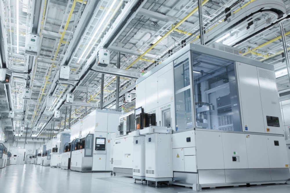
EG: We have a lot of fab space, over 12,000 metres squared of fab space, and it’s 200 millimetre, 300 millimetre, and also some specialty fabrication areas. And those are used multiple ways, but it is a functioning fab.
One of the ways that Imec netzero is used is we can run a process flow, identify what the big contributors to emissions are and then specifically target what we like to call improve projects on those sectors. For example, if it’s a fluorinated gas etch, we can specifically target projects that look at replacing the fluorinated gases (with their high global warming potential) for less impactful options. So that’s one of the tangible ways Imec netzero plays with the fab space we have at Imec.
PA: And you use that for your internal research, or do you also have outside organisations ask to use it and you work with them on anything they’re looking at?
EG: Both. I mean, Imec is a research institute and there are a huge number of partners as part of our ecosystem. So it’s definitely both some internally owned systems and projects, but a lot of them are collaborative because ultimately our mission isn’t just to identify a solution and keep it to ourselves. Our goal is to identify a solution and propagate it throughout the industry so that we can all reduce our emissions.
PA: One of the main reasons we’re having this discussion is that you’ve fairly recently developed a virtual fab as part of your Imec netzero modelling platform. It would be good to understand where that idea came from and what is the objective?
EG: That is the netzero virtual fab. You can almost use them interchangeably, so it’s really just a question of how you put the software together. I mean, it all relies on these calibrated models with a combination of supplier input and measured input to identify the emissions associated with a certain process step, and then strung together, they become part of a whole fab. In the virtual fab, of course, we have to add things like timing, idle time yield, a lot of complexity can get added on, and the software is pretty flexible in terms of being able to choose what you include or don’t include, even abatement options. There are different ways that people deal with emission output from tools like gases and those models can be changed. Also, there’s a lot of flexibility within this system so that if we have a partner as part of the programme, who wants to run their own use case, they know certain things about their yield and die size fab timing, they can modify it at as they choose.
PA: And using this modelling platform/virtual fab tool, IMEC and partners have been able to quantify the ‘environmental impact of patterning-related process steps for various logic technology nodes’? Or is there more to it than that?
EG: There are logic nodes, but we can do NAND, we can do DRAM, you can do multiple different types of devices, so it’s not just logic. A lot of the same background is there if you think about it, it’s a virtual fab that can make different things and you just have to modify the flows in order to get there.
PA: In terms of what you’ve been able to do with the virtual fab tool so far, what have you discovered, for example, to do with lithography and etch carbon footprint? You’ve got some interesting results, is that right?
EG: Yeah. So I’m from the patterning area, that’s my technical background most recently. I am part of the sustainability team but definitely targeting to improve different processes within patterning.
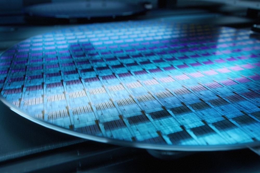
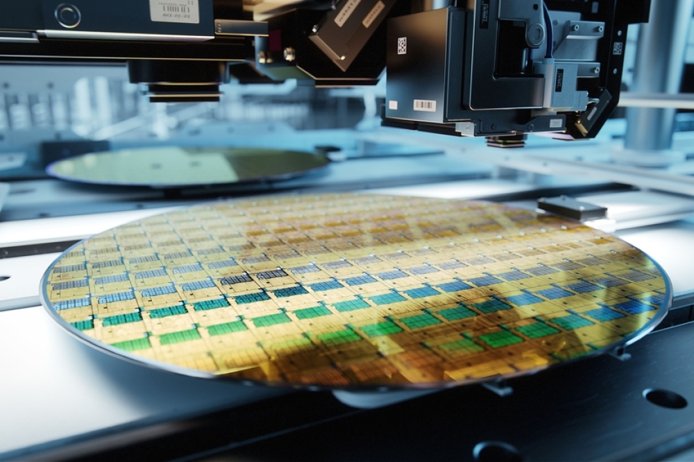
If for example we focus on a future node, you can see that I think for an N3 Wafer, it’s almost 40% of the influence comes from just patterning alone.
So, etch and lithography. We really targeted that area. In terms of lithography, the types of things you can do, we wanted to know. For example, if you go from DPV multiple patterning approaches to introducing EUV, which if you look and just compare DPV tool and an EUV tool, the EUV tool uses a tremendous amount of energy. It’s a complex source with relatively low efficiency to get the EUV light. And there was a lot of concern about introduction of EUV and manufacturing and what that would do with two emissions. So we did that comparison. But what we find is, for example, if you use N7 with and without EUV, the version with EUV eliminates a lot of extra process steps that are related to using multiple patterning approaches. So yes, you introduce this really high emission system but you eliminate a lot of etch steps, a lot of clean steps, a lot of deposition steps and in the end you actually have a lower emission fabrication process.
So that was one good example. We’ll be doing that sort of activity again when we talk about moving towards High-NA, which is even a different throughput model and something else we’ll have to look at for etch, there are other things to look at. For example, what can we do to optimise the etch stack in order to minimise the etch processes or to optimise there’s a lot of detailed process work that can be done on etch. And it was really helpful for us to identify it as a big contributor. Especially the high GWP gases are something that needs to be addressed in order to get the etch impact lowered.
PA: You described there the overall net benefit of the EUV process. But I think you’ve also done some fab experiments around lowering the dose of EUV as well. What results have you got with that?
EG: Yeah, so for example, you can just run a curve that shows what the impact of changing dose does. And there are a lot of different ways to address dose. And reducing dose also reduces cost. You have a certain tool with a given throughput and if you just lower the dose your throughput during the process time is going to increase linearly with that. So it’s a pretty obvious knob to work on and one that helps cost as well as emissions very easily. But it’s not so simple to get equal performance at a lower dose point. So some of the kinds of things you can do is use different resists, different bakes. So we look at all of those things and what we’re doing now is we basically have a calculator that we can apply to different projects just to see what the benefit is when you change dose, for example.
PA: Okay, so the ultimate there, you’ll produce, as you say, some kind of table or best practises so people can understand all the variables. Obviously, you need to produce a product - that’s important, but also you want to minimise or optimise your environmental footprint. So, it’s helping people understand the consequences of what they do or don’t do during the manufactured process?
EG: Right. So for a long time we’ve talked about PPAC, right. Power, performance, area, and cost, those have been things the whole industry has optimised around. What we’d like to do is add E for environment to that. So PPACE, and just like you said, just being sure that during the development phase we’re optimising for emissions as well as everything else. It’s an innovative industry, we can do this, but we have to know what we’re measuring.
PA: And in terms of the partners, I believe you’re able to share, for example, you’ve been doing some work with Edwards, so it’d be good to understand how you’ve been working with them and what sort of area helping them, collaborating with them?
EG: Yeah. Edwards is a great example of sort of an improved project. One of the consumables on the scanner for the EUV scanner is hydrogen. It’s used as a gas to keep the source clean, to keep the reticle environment, mini environment (RME) clean because it keeps carbon build up so that your mirror reflection stays as high as you need it to. So again, helping throughput. It also keeps particles away from critical areas in the source. So there’s really a tremendous flow of hydrogen through the system. And what Edwards has developed, they’re a vacuum and abatement company, and they have developed a system that actually reuses the hydrogen.
So rather than just consume it and then abate it with a common way suchas burning with methane, which is a high GWP gas and a pretty consumptive process, instead they’re recovering. And we had the first demonstration of that system in fourth quarter of last year at Imec and demonstrated a 70% recycling of the hydrogen. And going forward, we anticipate as much as 80%. Some changes are being made now to look at that. So, a really nice example of an abatement improvement that can really reduce the emissions associated with using EUV.
PA: Is there anything to add on the load? Because I know you are doing lots of work on the low dose solutions for EUV Lithography. Again, is that with partners or is that more of your internal research?
EG: A lot of the dose reduction projects are actually together with ASML. They’re one of our big partners there, but then almost every resist supplier is aware of this challenge and there are different formulations looking at that. So, I would say a lot of those dose reduction work is together with partners, various kinds.
PA: And I also believe the work you’ve been doing, you’ve identified etch directions for improved sustainability. Can you explain how that works as well?
EG: Yeah, so I think I touched on a few of them, but maybe just to say them all at the same time. So you can do things like optimise your recipe for having less power, more efficiency in terms of the use of the gases that you use, optimising stabilisation steps. If you really look critically at an etch recipe, there a lot of knobs that can be turned to minimise either the power consumption or what’s more important for etching is what we call the scope one emissions that are associated with the GWP gases. Those are, I guess, the biggest things.
One of our big thrusts this year is working on various ways to have what we call reducing the fluorinated content of the gases that are used in etch. So that’s basically reducing the GWP. There’s an output side of that which is working on abatement too. And that’ll obviously be considered with any etch process that we change. Etch is complicated, so there are a lot of pieces that come into it. And of course, we need to maintain performance at the same time as making all these other changes. But there are some good examples of effective work in the industry and we’re trying to bring more of those, optimise them and bring them to people’s attention.
But we’re not alone in working on this. There are a lot of companies both material suppliers and edge tool suppliers that are also working in this area, which is good because it’s a high impact area.
PA: To characterise it, is it very much trial and error? You tinker with a certain parameter, do you then anticipate a result and it tends to come as you expected, or is it often unexpected? So, it is very much you’re a bit in the dark, trying bit by bit all these different recipes, if you like, or do you have a fairly good idea of what you think will work and then you use the virtual lab to just say, yes, what you thought was indeed correct?
EG: The virtual lab is helpful to a point here, but we do need to make measurements as well, because the input gases, you could understand right away what the embodied carbon of making a certain type of gas is and how much it leaks and guess at what the output would be after etch. But in fact, you really need to measure. So this is one of those cases where you might have a relatively good idea, but measuring the by-products after etch are really important because some processes are very efficient consumers of the greenhouse gases.
And if that’s the case, it’s much, much less of a problem than if they’re actually being released into the atmosphere. And also, I should mention, my background was not etch until recently. I’ve been focusing on it more because of the sustainability work. So to me, plasmas are a little bit of a black box. I think that’s the way most people look at them. But perhaps if you had someone who grew up in plasmas, they wouldn’t think about it quite that way.
PA: And the overall objective is that you can get to the point where you can produce a semiconductor process flow with the sustainability angle, very much part of it. Do you have a time frame for that and how is your work going towards that overall goal?
EG: Our initial goal was to create this virtual fab or Imec netzero platform, so that you could actually measure and assess where you are today and then work from that. On terms of being able to move the needle of HVM manufacturing that relies on adoption and changes within the industry.
So our big goal there is really just to collaborate and partner as much as we can. For example, we are part of some larger organisations as well, such as SEMI’s SCC, the Semiconductor Climate Consortium. We’re heavily involved there and with other groups like IRDS, because I think climate is one of those things, no one’s going to be able to do it alone. And what we can do is try and look for the biggest gaps in the industry and try and fill them and sort of act as a way to propel everybody to a state where we’re using less and emitting less. But Imec could have a perfect process and if it’s only at Imec, it doesn’t help anybody.
PA: Just to restate, the fundamental issue is you’re trying to maintain and develop patterning processes for the industry moving forward, but at the same time reducing CO2. So to a certain extent they might appear, on the face of it, sort of incompatible goals. But your idea is obviously to make sure that the industry progresses, but it also reduces its carbon footprint – achieves much more in terms of sustainability.
EG: Exactly. I don’t think the industry would accept a process that wasn’t at a high level. They wouldn’t accept, for example, higher line edge roughness or lower EPE just because you reduced emissions. They want everything. But I think if we do this at the early stages, that’s possible.
PA: More generally, in terms of the industry’s outlook on sustainability - I think we covered earlier on the fact that, although 2050 is where most of the world’s headed, you say that some organisations are working to a much tighter deadline. A lot of industries, they started paying by lip service, a bit of green washing and then at some stage they actually started getting really serious about sustainability. Is that the same with the semiconductor industry? And do you think they’ve now fully understood their sustainability obligations or is there still a bit of a mixed picture as to companies that are at the forefront of it and others that are perhaps dragging their heels a little bit? Because it’s obviously, as we’ve discussed, a complicated process to understand how you can become green at the same time as carry on doing what you’ve always done in terms of the manufacturing?
EG: I think when you think about most companies, there has been a shift in that, in order to meet these net zero targets on a realistic timescale, it’s not just what the company itself does, their scope one and scope two emissions, it’s also scope three - what comes into them and what leaves them. That’s also going to be part of the equation and for that to happen they need to push on everybody throughout the supply chain. So now you have this pressure that’s coming from companies who have made these very public commitments, who have pressures from their communities to do it and from their customers. It’s becoming a lever on costs or getting business to actually have a green portfolio.
I think just lately there has been a shift in this way and that making the low emissions decision is also going to be good for business. I think when that happens you’re going to see an accelerated rate of change and I do see it already that some companies have been working on, for example, greenhouse gas replacements for ten years and now all of a sudden everybody wants to talk to them.
I do think change takes time, but I think the pressure is there to change more quickly now.
PA: And when it comes to achieving that, are you optimistic that the industry can improve and continue to meet the increased demand for the product as the digital world explodes and also meet every sustainability type?
EG: I guess I’m hopeful. I am worried about greenwashing. It is something like how do you make sure that we report? But I think that’s one place that standards from larger groups can come in and help, perhaps. And I do think it’s possible that we’ll have to compromise at some point. But I do see the pace accelerating, I think we’re moving in the right direction.
PA: Finally, when it comes to the external pressure, you say obviously big corporations sign up to ESG goals and they push down on the supply chain. But do you think it’s inevitable that there will be the need for government legislation or do you think the whole industry can collaborate better and more quickly to make sure that they try and stay ahead of what government might be asking? Or do you think there will be a bit of a crunch time when legislation comes in, everyone looks at each other and goes, heck, what are we going to do? How are we going to meet that?
EG: Well, I think the interesting thing about the global industry that we’re in is that different governments have come in at different times on different pieces.
For example, PFAS legislation has been a little bit faster in the US with 3M, so we haven’t talked about PFAS because it’s not directly emissions related, but it’s the forever chemical. And there you can see what the impact of legislation has on not just the US companies, but all companies.
I do think that it helps add this fear of legislation coming and we need a solution in place and we’re going to have to ask for exceptions and it might not be granted and then what will we do? So I think it’s helpful. I think the more we can have government legislation,
in addition to the corporate pressures that already exist to be green because of consumers and customers, I think that’s all going to help. So I guess I think it’s both. I think sometimes companies can act a little more quickly than governments, but when a government speaks, it carries a lot of weight.
PA: And just on that point, do you think there will be overall a fairly level playing field or, as history shows us, a lot of manufacturing sectors have been quite agile. To put it bluntly, they’ve moved where they can perhaps escape certain regulations and carry on doing certain things. Do you think there will be any hiding places for the industry should they wish it? Or do you think there’ll be pretty comprehensive, globally agreed legislation that will mean that they can’t run away from their obligations?
EG: I have trouble imagining that all of the governments will agree to putting in place the same legislation at the same time. I like to think that customers will not welcome companies hiding from emissions regulation, but I don’t feel equipped to say that it won’t happen.


