The perfect partner for wet process equipment?
TOBIAS BAUSCH, CMO & CTO AT AP&S INTERNATIONAL, discusses with Philip Alsop, SiS Editor the company’s batch processing, single wafer processing and support equipment technologies, with the emphasis very much on continuous innovation to deliver cost-saving, operationally-optimised and sustainable customer solutions. The conversation also covers some of the current industry challenges, including ongoing supply chain issues and skills shortages, as well as the opportunities offered by new and emerging markets.
PA: The obvious place to start would be if you can give me a little bit of background on the company, the history and some of the key milestones.
TB: The company itself, AP&S started in 2003, but the history starts in 1995. The current shareholder, Horst Hall, started the business in 1995. Then, from 2001 to 2003, we were part of the SEZ Group and we were called SEZ Germany. The batch part during this time was that SEZ Austria had a single wafer portfolio and in 2003, Alexandra (Laufer-Müller) and Horst, the current shareholders of the company, did a management buyout and founded the company AP&S. So, as I’ve tried to explain the history is much longer than 2003. Which means this year we have the 20 year anniversary. In July we celebrate this with the company employees and the partners.
And yes, over the last 20 years we developed several tool platforms, mainly in the wet process sector. So all our machines are used in the wet departments of our customers. And during this time, sure, we have several milestones - we invested in an in-house lab where we can run demonstrations for customers, the demonstration lab starting in 2012. And as I said, over this time we have a lot of redesigns or redevelopments of machines, new developments of existing machines or new machines.
PA: And it would be good then to move the actual technology solutions you provide. If you can run us through the batch processing solutions - one of your main sort of strengths?
TB: We have the existing three platforms, it’s the batch, the single wafer and the production supporting equipment or facility logistics as we call it. And the batch is this one where we’ve grown up. Since 2003 we’re starting with the batch tools. We have there several platforms, semi-automated and fully automated platforms. The smallest platform is a two-tank solution where customers can have etching and the cleaning application in one equipment. And mostly this tool will be used by customers who coming from manual operations - where the operator handled the wafers manually and they want to go to some kind of automated production. And the next platform is a tool which is called multi or giga step. It’s a bridge tool. It was developed in the 2009-2010 years and we have the possibility to run in these platforms very easily, six and eight inch in a bridge combination without any kind of modification between the wafer sizes. So at the moment this will be very requested related to the Silicon Carbide issues and the Gallium Nitride request. And this tool platform itself is very modular and flexible.
So the customers could also decide by today to go with a tool configuration for a cleaning application and, in the future when their needs change, the product is changing or whatever, we could reconfigure easily, by adapting the modules or insert or disassemble modules or insert new models, the tool configuration. So that’s one of the key benefits of this platform.
And then we have a high throughput platform, a new development - it’s called Nexus Step. It’s up to 12,000 wafs per day, mostly for cleaning applications. We run in this case with 100 wafer batch per load. And therefore we have this year within the year, by end of the year, let’s say we will have the market launch of the Nexus Step, which is a new development. But I think we discuss later on about developments more in detail.
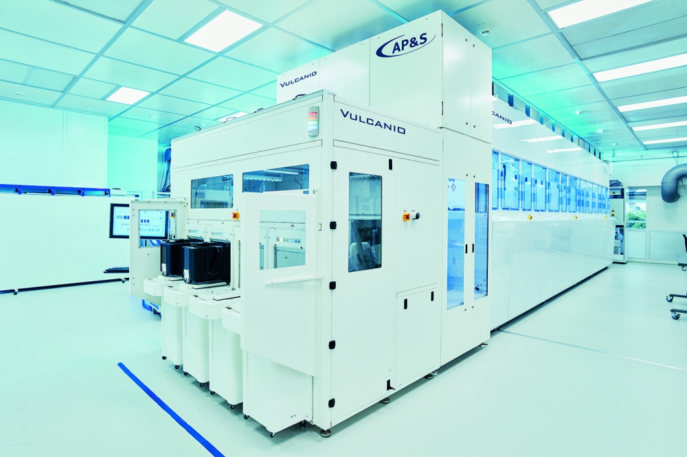
And last but not least is a very special tool. It’s eless metalization equipment for underbump metalization, we call it Volcano. We start this development in 2009. And I think by today we are at most of the customers in Europe. The process of record for this eless metalization, where we can have nickel, palladium, gold metalization on copper or aluminium pads and, yeah, this tool platform was one of the biggest success stories in the history of AP&S.
Our target is to have a clear enlargement of the bath lifetime, because the eless chemistries are quite expensive compared to standard chemicals in the semiconductor industry and we want to ensure that the customer can run on a higher throughput base on a better total cost of ownership.

PA: We can perhaps go on to the single wave of processing technology - if you can just outline what it is you do in that area.
TB: The single wafer equipment we developed in the early 2010-2011 years. And as I said, we also decide very fast to go with the single wafer in a demo application to show the customers the possibilities to run demonstrations. And in the meantime, we run not only demonstrations, we also run R&D activities in the lab.
The tool itself is a very small equipment. We can start with one chamber. It’s called a single chamber. We could adapt it with a robotic module to have automated loading of the wafers or the masks and up to a double chamber. So, the biggest enlargement of the tool configurations are two chambers, a double chamber solution. But in the chamber itself, we are not limited. So, we could run up to twelve inch on the wafer base and up to nine inch on the mask size. And, during the development of the machine, we decided to give the machine the name of the processes. So, for example we have a spin mask which, as the name suggests, that’s the equipment for the mask cleaning a spin lift off. It was designed for metal lift off applications or spin RCA spin scrubber for typical cleaning applications or spin metal or spin edge for etching applications.
And each of them has specialties and different features related to the processes. For example, the spin metal, we developed for a metal etch application, an endpoint detection system which is included inside of the process chamber. And therefore we had in this case, one example we had developed with a customer realised for three metal layers, so they had a metal layer of silver, nickel and titanium. And with this endpoint detection we could realise a very fast step, very fast process steps.
We can reduce clearly the undercut and the over etch and especially we can compensate any kind of chemical concentrations, temperature variations in the chemistries, over the time of the chemistry usage, dilution or degradations. So, all these things were compensated even if we take a look on the etching endpoint. And this was, for example, one of the benefits we could include in these single wafer chambers. As I said, there are a variety of features related to each dedicated process step.
PA: It sounds what you described there, that you collaborate quite closely with customers. So, I guess you produce what we call a standard range of equipment solutions, but then you will work with individual customers to customise them for their specific needs?
TB: Especially single wafer or even on the batch. I forgot previously to mention that we also include in this demo centre four years ago a batch demonstration equipment. And this is what we see. So, as I said, we do a lot of R&D activities with the customers. So they come to us. They have a dedicated problem. Sometimes they could not solve it in their own facility, related to contamination issues because they are not allowed to run different tests on production equipment or at the moment, for sure they are all fully loaded, so they don’t have the time to do a lot of R&D activities in their own production lines. And then they came to us with the wafers, with the issues and we do together the R&D activities in our lab, find the best set up, or even find a new set up with new features like ozone, like megasonic, supporting whatever. And then at the next step we try to implement it on the existing machine of our customer site. Or if for sure needed, we will develop a new machine for the customer itself and we build it. During the manufacturing phase we try and we go ahead in the lab to bring the process as close as possible to a production running parameter set up.
PA: Okay. And you mentioned as well at the start that you make a range of support equipment. So again, it would be good to understand support equipment - what does that actually mean?
TB: So, the supporting equipment or we change it to the new definition in the near future. Fab logistic equipment is the third pillar of our product portfolio. In this case it includes also cleaning equipment, but especially for carrier boxes, SMIFs and FOUPs in this case, or parts or tube cleaning equipment for parts made of quartz parts and chemical delivery systems. So, I think this is the basics. Every fabrication needed to run their production and especially on the carrier box or SMIF or FOUP cleaning, we see in the last years a very increasing demand for sure, the ramping of every customer is ongoing. And if you have more wafers in the facility or you’re producing more wafers, you need more boxes. And these boxes have to be cleaned. Therefore it’s clear that the customers need more cleaning equipment. Also we could generate and provide to the customers a clear benefit if they go back to in-house cleaning. In the industry in the last ten to 15 years, several of the customers don’t want or don’t do this in-house. So, they outsourced their boxes, their FOUPs, their SMIFs to external cleaning centres.
But, at the moment, we see the benefits bringing it back in-house. You have faster reaction time, you have a higher flexibility when you have to clean boxes or FOUPs immediately. You could reduce logistic costs, you don’t have to send it out to an external provider, get it back and so on. You lower the number of parts which you have to have in the loop for the cleaning and at the end for sure, reduction of the cleaning cost, something which can be calculated and visualised. And I think what will be more important in the next years, the carbon footprint could be much better because you don’t have to send parts on a longer logistic way to the external partner. As I said, you can reduce the logistic cost, but you also can improve your carbon footprint.
PA: And in terms of the applications, I think you referenced the main ones. You’re focused on a number of application areas, cleaning and etching would be the main ones. Were they there others as well? What are the focuses exactly?
TB: Yeah, so these two are, I think the typical ones, which we are coming from and which the company history was grounded on - typically cleaning machines in the front end production for pre-diffusion cleans or post CMP cleans, whatever, on the etching equipment for the typical front end steps for oxide edge, nitride edge, silicon edge and so on. So, this is the basis where we found our tool base, where we found our process know how and so on and over the last year are several things coming add on. So, especially solvent applications was very important over the last years and I think AP&S was one of a few worldwide which include solvent applications in machines where we have a tool configuration in parallel also with acid steps or cleaning steps. So especially these things, solvents and so on. You have to know what you have to do related to the security issues and so on. But that’s one of the additional focuses and applications we do. The metal etch I explained previously on the single wafer, in the meantime where we had developed this single wafer metal etch with the endpoint we also go ahead and do this development on a batch platform.
It’s on our multistep and gigastep tool platform to upgrade or enlarge the throughput capability on the batch tool. Everybody is clear on the batch tool. You will have a higher throughput application possibility compared to a single wafer. Both types of equipment have their benefits and pros and cons. But especially the metal etch was growing over the last year. And yeah, as I said previously, the eless metalization, this is one of the most popular applications we focus on at the moment. This is also coming for sure from the mega trends we have at the moment with the decarbonization, green energy, electrical cars, loading stations and so on. At the end everybody needs power devices. On the power devices you need a good metal stacks for the UBM, for the under bump metalization. And we see also here that these metal layers where we can realise with the eless process steps are very good in the terms of quality, temperature and so on for these new technologies here.
PA: As you’ve been answering, you’ve alluded to a lot of the technology solutions and clearly some innovations along the way, but are you able to summarise some of the recent innovations or at least highlight some of the most important ones as far as you’re concerned, what you’ve been developing recently?
TB: I think I can summarise, let’s say, three of the main innovations we do at the moment, or we have done in the last two years. We hve a very huge in-house software department. The company has 250 people, but the in-house software group is compared to this number, a huge group. And we do this with a clear strategy to have it in our own hands, to have the development of the software in our own hands, because we also see that software features, interfaces to customer interfaces, handling solutions and so on would be the key in the future. So, we speak about AI, we speak about predictive maintenance and so on. All these things are related at the end to a software feature so that the tool can control itself, measure itself, do the diagnostics itself to see if a part, even a pump, a heat or whatever is coming to a failure and so on. All these things are related in the software, in the software code and therefore we do there, let’s say a lot of investigations and innovations.
Also what is clearly focused, but that’s nothing new that’s in the industry since it’s been happening for quite a while, is the quest to increase and optimise the throughput of the machines so you can even lower the cost in the production - if you can optimise this throughput you can reduce process times, can save chemistry costs or in this case also it would be in term of a green footprint of the company a good feature to save chemistry volumes and costs.
So, this is something we take account of in the software.
The second is the next step where we are in the development phase of actually building a new machine currently. This will be the machine especially designed also for a high throughput eight inch application. We will have inside of the machine a unit to stock up to 44 transport carrier or boxes. And it allows us to have a very flexible handling of it in terms of recipe control and throughput control. And it allows a customer also to stock carrier boxes and so on inside the equipment and can bring it to the equipment in a time when the time is available and we use it, we stock it and we give it back to the fab when the production or the recipe is finished.
And this is a tool, as I said, with additional process features. We’re reducing some process activities like for only one example, reduce the rinsing time to save time and to save also money and to save at the end DI water which also be good for the whole environment on the customer side.
And the third is our cleanser. It’s the equipment we developed over the last two years. It’s a new cleaning equipment for fab logistics and especially for cleaning off FOUP. The equipment is able to run twelve FOUPs per run. And we see that we have time or a recipe reduction from approximately ten minutes to benchmark equipment. So we also could increase here the process sequence and enlarge the throughput at the end. And this equipment is developed with the implementation of automated loading system. So, especially on high automated twelve inch fabrications, we see that the demand to load the machine not by an operator, so to load the machine by overhead transport system is also coming in the path cleaning area. And this is something we focus on. And the development of this fully automated loading system is ongoing. And I think we will come out with the market launch in the next one and a half years.
PA: A lot of your success is clearly based on the people and the skills you have within your organisation. And I know you pride yourselves on your recruitment and skills development. It’s very important to the company. So particularly, I guess at the moment where all sectors are maybe struggling a bit, but the technology sector, we constantly hear of skill shortages. So, what sort of initiatives do you have in terms of both identifying suitable people to join yourselves and also then once they’re in the company, how do you help them to develop?
TB: Yeah, so in the south of Germany, when we are located close to the Swiss border and to Lake Constance, we have for a good location for employees. We have a lot of strong companies and all of these are looking for high qualified and good people. So, for the company itself, as you said, it’s quite difficult to find the right people. We could say that in the last three years, during the pandemic situation on the R&D sector, we find very good people. I think there was the situation that a lot of people from the universities who were finished with their study were looking for new jobs and not everybody was hiring new people at that time. We decided decide early on that we would use this situation and get a lot of students into in the company. So, on the R&D sector we have a better situation compared to the manufacturing area. In the manufacturing area it’s quite difficult to find the people to produce the machines and therefore I think it would be the biggest challenge over the next years to find there the right people and the people with the good skills and the right skills.
We also try to hire people who come from industries closer to the semiconductor industry, to the machine manufacturing industry. We have a lot of machine manufacturers around of us which are in the metal sector.
Internal study and training is one of the biggest things we do. So, we have in several departments, trainees and most of them, or let’s say all of them, will be after their training time and after the study time, part of the AP&S team. We do this very carefully and I think we have at the end, if they are finished with their study, we have several options. They could start in an R&D area or in sales or marketing, and if their technical skills are quite good, they also can start in the manufacturing sector.
PA: Do you think the industry has more or less recovered from the impact of the pandemic? And if so, or whatever the current state is, what sort of opportunities are there, and are there still any sort of challenges off the back of it? Everyone’s calling it where we are now?
TB: Yeah, that’s a difficult question because I think over the last three years nobody was able to say what happens next. So I think at the beginning, 2020, everybody was afraid and nobody know what’s coming soon and then I think especially the semiconductor industry was at the mid tp end of 2020, very fast in a way and since this time everybody is growing and ramping up. If it’s going back to normal, I don’t know. At the moment we see that the parts we need out of our own industry, plc controller, motor controller, whatever, still have a lead time of 50 weeks, so approximately one year. On other parts we see the lead time was also in the past close to 52 weeks and they’re going back to 44, 42. So there we see a reduction but especially on the electronic parts we doesn’t see a clear reduction. Therefore, I don’t know if we are back on a normal level. We see that the demand for semiconductors also relates to a higher demand of equipment, which was for us measurable in the order entry we have had over the last two or three years and for sure also this is also related to several megatrends.
We have the emobility, decarbonization trends and so on. And if you take a look at all this market research it seems to be that it’s going on this way, especially the power industry, power semiconductors will grow more than others - but what is the new normal? I don’t know.
I think at the moment, especially industries and ecosystems like Europe, like Germany, like other European countries. We see that the globalisation, which we have prior the pandemic was very good and great and it was not a problem to have a supply chain which is around the world. I think in the semiconductor industry the supply chain was typically around the world and it is clear for everybody. And then we have this pandemic situation and this crisis, and then everybody sees, okay, the supply chain was cut. And at the moment, for the European people, it’s interesting and great to see that we have a lot of new projects. A lot of new, growing fabs, even internal, coming to Germany. Infineon decides to expand, TSMC, was in discussion to have a new fab in Germany or in Europe.
And I think it’s great, but I don’t know if this would be the first step to have towards the decentralisation - to the external production coming back to internal production on each continent. If we are back to a new normal. I don’t know. I think we will have also a lot of movement in the market and let’s see what happens in the next three years. So we had now three years Pandemic time and I think it takes minimum the same time to see what is the new normal.
PA: Are you able to analyse what sustainability means for the industry and particularly the supply chain and anything around the sort of geopolitics as well?
TB: In terms of geopolitics, I’m not a politician, so the geopolitics situation is quite difficult and two years ago nobody believed that we will have a war in Europe now we have it so what happens in the next three years? I think it’s quite difficult to underline this.
It is important in the semi industry to have a strong network and also to know and have scenarios, backfall scenarios - what happens when such situations came or what happens when such situations don’t come about.
On the sustainability view, the resources we have are not endless. So, if we take care about the materials if we take care about raw materials or especially on the employees and the technologies we have to find ways to improve what we do, so to handle the resources we have. Even if we speak about water, which I believe will happen in the next years, one of the most important resources around the world, I think it will be difficult in the next years around the world to have it in the right volume and in the right quality.
And our industry is one of the industries which need a lot of them. And I think this should be the target to focus on activities, to save these resources - raw materials, water, whatever. And this will be also the success in the future. These companies which find a way to handle these resources in a good way, which are going on a sustainability strategy will be successful.
PA: Are you noticing that your customers are more interested in sustainability? When they’re talking to you do they ask about your sustainability initiatives and your supply chain?
TB: We’re getting these questions more and more. We are part of several sustainability projects. Even if you have at the moment we have customers which have fabrications which are 20-25 years old, and for sure they will run these fabs for more than the next 20 or 25 years. They have clear communicated sustainability strategies. And for us, it’s clear as a supplier of this industry to go ahead in these strategies, to find ideas and ways to come in close to the targets which the customers have and find our own way, our own ideas to fulfil this sustainability request from the customer sites.