Loading...
News Article

Chiplet Summit 2024 shows how advanced packaging keeps Moore’s Law alive

News

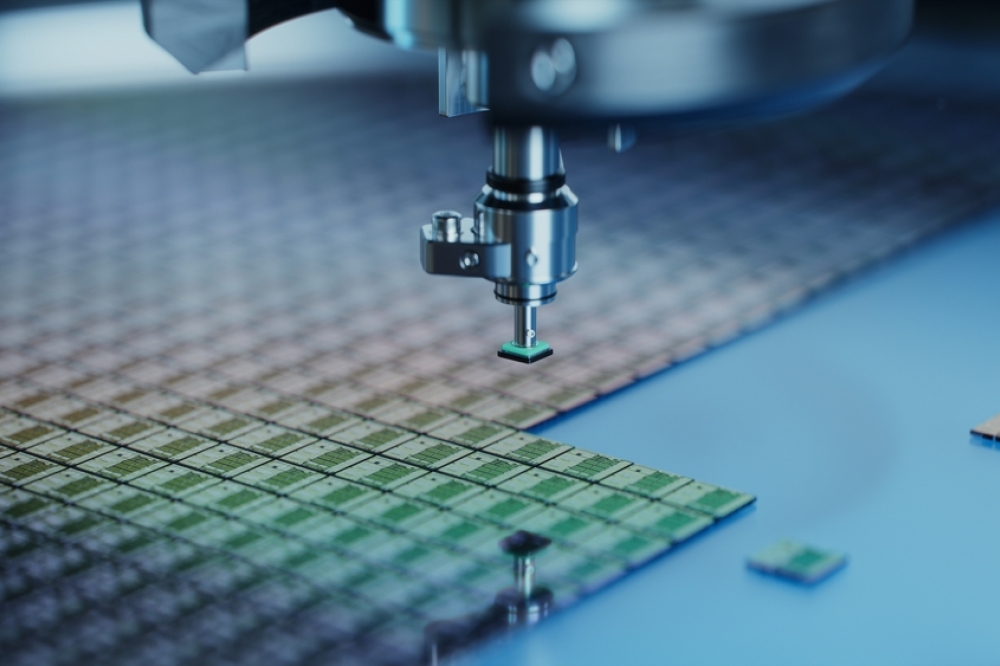
Smaller design nodes are now far more costly and much harder to achieve. So interest has turned to approaches that do more at the package level.

Chiplet Summit helps educate both design and packaging engineers. The advanced packaging tutorial covers methods such as 3D, wafer-scale, and panel-scale. The Working with Foundries tutorial then shows how such approaches have become part of manufacturing. Later sessions deal with finding the right package for an application, as well as short-term and long-term trends.


The Summit also offers major company keynotes, expert tables, panels, and paper sessions. An exhibit hall has key products from industry leaders.


“Chiplet Summit helps designers profit from major advances in packaging,” said Chuck Sobey, Summit General Chair. “Designers and packagers can both learn how to develop SiPs (systems-in-package), use die-to-die interfaces such as UCIe, and create supercomputers in a package.”

North Carolina State University orders Ion Beam Etching Equipment
TD Shepherd joins Silicon Catalyst
Physik Instrumente aims to triple capacity
Chiplet Summit 2024 shows how advanced packaging keeps Moore’s Law alive
Infineon introduces the XENSIV PAS CO2 5V sensor
SiMa.ai expands ONE Platform for Edge AI
An industry game-changer?
Intel names new representative to Si2 board
Faraday unveils advanced packaging coordinated platform for multi-source chiplets
Xenics Expands Its Advanced Imaging Portfolio
IDTechEx looks at sustainable helium use
Compact industrial 3kW programmable power supplies
PCIM Expo 2025 even bigger to meet growing demand for power electronics
Xiphera develops quantum-resilient hardware security solutions for space
Advantest to showcase IC test solutions at SEMICON India
ASMPT and TATA Electronics Private Limited form strategic partnership
Singapore and India sign MOU on semiconductor ecosystem partnership
The Netherlands expands export control measure for advanced semiconductor manufacturing equipment
Tech industry veteran Anders Storm named CEO of Dirac Research
Testing time in Taiwan
Electro Rent unveils large facility in Mechelen, Belgium
AEM expands system level test on AMPS Platform
Absolics turns to Solace
ACM Research receives orders for wafer-level packaging tools
En route towards the first German quantum computer
Element Six wins U.S. Department of Defense UWBGS program
ACM Research expands Fan-Out Panel-Level Packaging portfolio
Precision sealing for advanced semiconductor manufacturing: Greene Tweed leads the way
Electroninks launches Copper MOD Ink
Advanced thermal control techniques to improve wafer manufacturing yield
Advances in active alignment engines for efficient photonics device test and assembly
Automation in semiconductor test processes: a key factor in modern production
×
Search the news archive

To close this popup you can press escape or click the close icon.
Logo
×
  • 1st January 1970
  • 1st January 1970
  • 1st January 1970
  • 1st January 1970
  • 1st January 1970
  • 1st January 1970
  • 1st January 1970
  • 1st January 1970
  • View all news 22645 more articles
Logo
×
Register - Step 1

You may choose to subscribe to the Silicon Semiconductor Magazine, the Silicon Semiconductor Newsletter, or both. You may also request additional information if required, before submitting your application.


Please subscribe me to:


You chose the industry type of "Other"

Please enter the industry that you work in: