
Rudolph Unveils New Inspection Suite
Rudolph Technologies has launched two new inspection and metrology solutions for advanced semiconductor manufacturing: The Firefly System for high-resolution inspection in front- and back-end applications, and the Dragonfly System for high-speed two-dimensional (2D) inspection in advanced packaging processes. Both systems leverage newly designed optical and imaging systems optimized for defect type, size, and maximum throughput.
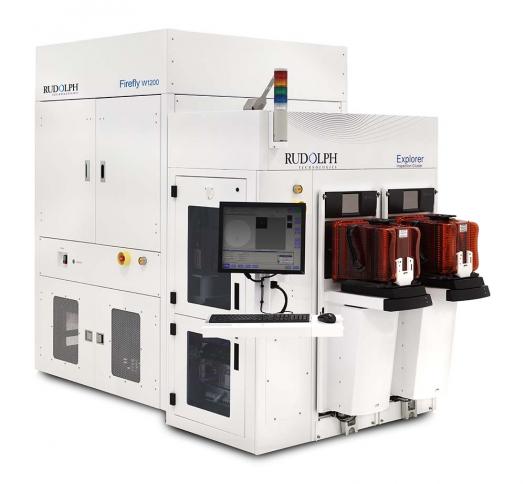
The new Firefly inspection and metrology system has been designed to detect defects smaller than one micron in multiple applications, including: fan-out wafer level packaging (FOWLP), CMOS image sensors, microelectromechanical systems (MEMS) and radio frequency (RF) sensors. Device manufacturers are facing challenges such as detecting faint residue on CMOS imagers, and residue on bump top and bond-pads that lead to field failures, but are almost impossible to detect using current inspection technologies. The Firefly system, configurable for either wafer (round) or panel (rectangular) substrates, includes Rudolph's recently-introduced Clearfind Technology, one of the multiple imaging modes designed to address these challenges.
Clearfind Technology is a patented technique for enhancing the detection of defects by fluorescing organic materials that often escape conventional illumination techniques and are a source of yield-robbing interconnect failures. The Firefly system's unique combination of defect sensitivity and substrate flexibility, in a single platform, reduces capital investment requirements and provides a reliable pathway to transition from wafer to panel-based processes. The system will begin shipping in September to key customers in Asia.
The new Dragonfly inspection and metrology system targets large die, multi-chip advanced packaging applications, with 2D inspection sensitivity down to two microns, a modular approach to integrated metrology and defect analysis software. This unique combination of technology allows the system to quickly detect, image, and analyse defects on a broad range of devices and packages. The Dragonfly system will deliver critical in-process inspection and metrology for wafer reconstitution, after develop, after etch and at each level of redistribution. Integration with Rudolph's Discover yield management system and automated defect classification quickly turns defect data into actionable process control, improves classification and reduces manual review. The system's new time delay and integration (TDI) based inspection capability has already been qualified for production by a major foundry in Asia. The Dragonfly 2D systems are targeted for shipment in the fourth quarter of this year.
"The Dragonfly system complements Rudolph's flagship NSX 330 inspection system by extending defect sensitivity and resolution for advanced applications on a platform optimized for cost of ownership," said Mike Goodrich, vice president and general manager of Rudolph's Process Control Group. "Flexibility and upgradeability are at the core of the Dragonfly system design, allowing Rudolph to respond rapidly to the next-generation 3D and metrology needs of our development partners."
"Automotive, mobility and the Internet of Things (IoT) markets are fuelling demand for low-cost, high-performance devices packaged in complex multichip modules. This dynamic has driven creative packaging approaches that mix and match various technologies and require advanced inspection and metrology for shrinking redistribution lines (RDL) and other interconnect features, as well as inspection for smaller defects and organic contaminants. The Firefly and Dragonfly systems offer our customers the most comprehensive and flexible inspection platforms available on the market today and reflect an emphasis on increasing our R&D cadence, while maintaining high standards of quality and usability," said Mike Plisinski, chief executive officer, Rudolph Technologies.


