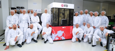
FEI Celebrates Shipment of 1,000th Helios DualBeam System


FEI has announced a milestone of the 1,000th Helios DualBeam system shipped since the product family was introduced in 2006. The 1,000th system was manufactured in FEI's Brno plant and was shipped earlier this month to a semiconductor customer who is utilizing the system for advanced failure analysis on sub-20nm semiconductor devices.
The small DualBeam (SDB) platform combines a focused ion beam (FIB) and scanning electron microscope (SEM) to enable industry-leading three-dimensional (3D) characterization, analysis and image reconstruction, nano-prototyping (fabrication and testing), and high-quality transmission electron microscope (TEM) sample preparation for both research and industrial workflows. Originally developed for semiconductor manufacturing failure analysis, the Helios DualBeam has enabled many new applications and is now also widely used in the materials science, life sciences and oil & gas industries.
FEI CEO, Don Kania, states, "The Helios DualBeam family has been a very successful product. We have sold more Helios systems than any other product segment in our portfolio, and it has been adopted by a wide range of customers, with varying expertise levels, across all of our market segments."
Throughout its history the Helios family has consistently led the field in performance and technological innovation. The most recent Helios platform is the 4th major revision in a decade -- a remarkable record for a major instrumentation system. Each generation has offered substantial improvements over its predecessor and competitors, including higher resolution SEM columns, higher current and lower voltage FIB columns, and new gas chemistries to provide unprecedented levels of imaging quality and operational capability.
John Williams, vice president of marketing, FEI, adds, "We've pushed the envelope in the semiconductor industry to keep up with ever shrinking IC geometries. For example, in November of last year FEI's Helios DualBeam was the first to market with a TEM sample preparation solution capable of making 7nm thick lamella, addressing the needs of our customers who are developing next-generation devices. This level of leadership has, in turn, catapulted the development of the DualBeam and our leadership in other industries. We introduced the DualBeam technology concept in the early 1990's, and FEI has continued to lead its technological and application development ever since."


