
Feature: Automating Cleaning Processes for Quality and Volume
The consistent purity of materials used to fabricate components of electronic devices can have a critical impact on their performance. For example, producing semiconductor-grade silicon used for electronic chips involves upstream cleaning of polysilicon chunks to a purity of has high as 11N, which translates to 99.999999999 percent. For photovoltaic applications such as solar cells, the silicon purity levels are not quite as high (5N) but critical to producing efficient photoeffect.
These and many other types of products used by the MEMs, biotech, LED panel and other micro-and nano-technologies that depend on uniformity that is provided by the repeatability of automated cleaning systems.
The cleaning process usually incorporates cleaning agents such as chemicals, an appropriate rinse bath, and a method of drying the material. Chemicals may also need to be heated and or product agitated to provide optimal cleaning results. An accurate means of measuring and dispensing cleaning agents safely and also safely transporting the products and materials being cleaned are required.
Manually operating a cleaning process calls for at least some worker intervention to precisely perform the above activities using a production system such as a wet processing bench. Because some cleaning processes require etching with harsh chemicals, worker safety is also a concern.
"Companies that choose to automate a cleaning process usually do so for one or both of two reasons", says Louise Bertagnolli, president of JST Manufacturing (Boise ID). JST designs and manufactures a variety of manual and automated cleaning equipment, including proprietary systems that include all of the features and transfer devices required for a complete turnkey cleaning process.
"The first reason is repeatability, the ability to precisely repeat a cleaning process, including the exacting measurement and dispensing of the cleaning agents and rinsing solutions as well as providing the systems and tools necessary to clean and transport the items being cleaned from one bath to another," Bertagnolli explains. "This ensures that all materials or products will be uniform in purity, and a "˜plus' benefit of worker safety is also provided."
The second reason some companies automate the cleaning process is to enable greater throughput for high-volume production. If the process takes place in a cleanroom, then the entire system including motors and robotics must be appropriate for that environment.
"There is also another class of semi-automatic equipment that enables automated process control, a built-in transfer system and other features on a relatively small footprint," Bertagnolli adds. "This type of system is an economical solution to lower-volume cleaning of such products as nuclear sensors, crystals, and polysilicon.
"
Ensuring successful automation
Customizing cleaning systems can provide high dividends, yet it is also a complicated undertaking and requires engineers and technicians who understand the individual needs of customers.
JST works with automation partners such as Bosch Rexroth (Charlotte, NC) to develop comprehensive wet-bench cleaning stations using linear motion and electric drive and control technology.
In a recent project the two firms worked together to create an automated system for cleaning silicon chunks to the extreme purity of 11N to meet requirements for the manufacture of semiconductor chips. The project entailed building a cleaning line 138 ft. in length and incorporating multiple gantry robots.
"The throughput volume requirement for these chunks was four tons for every 22-hour shift," Bertagnolli explains, "so we had to develop a basket system to transport the material throughout the application. The process included etch-cleaning and vacuum drying that volume, which was difficult because the chucks all had a variety of uneven surfaces."
To provide for such a long cleaning system, JST engineered and built it in two units. In the 24-ft-long unit, baskets of chunks are manually loaded through an auto-door. Then two-axis robots cycle the baskets through five acid etch baths and two rinse baths arranged in a single row down the length of the second unit.
Throughout the silicon cleaning process, protecting the components against contamination and pitting is critical. Yet, one on the unusual aspects of this cleaning system is that the first unit of the line employs overhead gantry, or Cartesian robots, which are not often used in semiconductor process systems to avoid generating particles over the product. However, after extensive particle testing in cleanroom conditions, the system proved to generate far fewer particles than the specifications allowed. Proprietary seals keep the linear motion rolling strips clean and prevent the chemical etch from pitting the linear modules. The system incorporated other features to ensure the system met Class 10 cleanroom standards or better.
JST and Bosch Rexroth also partnered on a "sister" project that involved the cleaning of silicon "seed rods" that grow the polysilicon ingots from which the chucks are made. The seed rod cleaning tool also utilizes a gantry robot to move the ingot-carrying cylindrical carriages through a sequence of etch baths. One of the keys to that solution is a custom designed fixture that rotates the rods in order to have them etched evenly.
"This rotational fixture also enables the rods to be cleaned to a very high purity," Bertagnolli notes. "We use a variety of rotational cleaning fixtures quite often, but also incorporate other designs and techniques as well "“ whatever will be most effective in getting the job done efficiently."
Bertagnolli advises that not every project is fully customized from the ground up. Quite often standard automation platforms can be customized according to length and height and number of baths. Cleaning process designers can consult with automation suppliers to determining where to put the transfer system and what automation modules will fit best in the space available,
The semi-automated system
Many processors with lower volume throughput requirements might consider semi-automated cleaning systems, which can provide the advantage of repeatability as well as other production advantages and added safety.
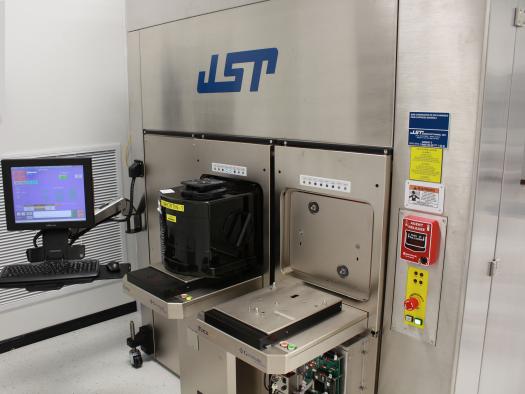
This type of cleaning system is appropriate for MEMs, LEDs and silicon applications. It is compact, software controlled and usually easy to service.
JST manufactures a standard compact semi-automated wet bench called the Tigress, a two axis, front-to-back compact system that is used by smaller semiconductor companies.
A dual version of this semi-automatic system is also available. It is popular among semiconductor manufacturers who use it for cleaning, stripping, and etching of semiconductor substrates who use cleaning acids and bases or solids to remove photoresists.
"These semi-automated cleaning systems are ideal for companies that are cleaning MEMs and smaller semiconductors. They are a very cost-effective means of automation," Bertagnolli says.


