
FEATURE: Reinventing the Spring-Loaded Probe Pin
For decades the spring-loaded probe aka pogo-style pin has delivered excellent mechanical and electrical performance in a highly compliant contact. However, this often came at a high cost given that each pin is constructed of 3-4 discreet parts manufactured and assembled in a laborious, less-than-fully-automated process.
The cost could be so exorbitant, in fact, that when significant volumes of pins are required, many opted to utilize less compliant, lower performance alternative contact technologies to reduce costs.
This approach is becoming less viable, however, with the increasing miniaturization of integrated circuits, electronic components and devices that pack more circuitry into smaller footprints.
A single test socket for reliability and burn-in testing, for example, can require hundreds and even thousands of spring-loaded probe pins in a fine pitch configuration. The same applies to board-to-board compression connectors. When factoring in multiples of test sockets as well as production-level quantities of connectors, pin quantities can literally run into the millions.
Enter, or perhaps re-enter, the spring probe. With a new approach to pin design and a complete re-invention of the manufacturing process, miniaturized spring probes as small as .2mm are now available that provide a high temperature, current and bandwidth performance pin at the price of a stamped contact.

Traditional Pogo-style Pins
Although designed and manufactured in subtly different ways, the pogo-style pin is typically constructed of a pin, two plungers and a spring encapsulated in a metal shell.
This style of pin is highly compliant, which means it is designed to compress or "comply" during insertion. This is critical when attempting to maintain a good connection despite potentially uneven surfaces, varying heights, errors in parallelism and flatness, or pivoting or rotating elements.
Although compliancy can be achieved by other techniques, such as bends, buckles, or cantilever-style contacts, additional space between pins is required during compression. Spring-loaded pins operate in a purely vertical fashion, so the maximum space occupied at any time is defined by its diameter. This allows for placement of spring-loaded pins in fine pitch distances as low as .2mm.
The trend toward more compact, high density electronics design "“ defined as the number of pins in a small area or the distance between pin centers "“ is already impacting several markets.
One market that regularly utilizes fine pitch spring probes is for electronics reliability testing, including burn-in, HTOL, HAST, THB and other testing protocols. To conduct this type of testing, sockets are manufactured to provide an intermediate (temporary) connection through an array of pins between the printed circuit board (PCB) and the components or multi-chip modules being tested. The PCB is then connected to a computer or other device for data capture and analysis to determine pass or fail.
The other market is compression-style board-to-board connectors used in electronics for telecom, automation, medical, aerospace, and military applications. These specialty connectors utilize spring probe technology to create a one-sided connector that is mounted against pads on the PCB. The benefits of spring-loaded connections include the elimination of receptacles to reduce costs, space savings, "one-touch" attachment and removal, and high durability.
Whether creating a temporary connection, such as for testing, or as a permanent board-to-board interconnection, the common denominator is more pins, less real estate.
"Devices used to have 2,000 pins in a two inch square area. Now they want the same 2,000 pins in a one-half inch square and the only way to do that is to reduce the pitch of the device," says Ila Pal, Chief Operations Officer of Ironwood Electronics, a manufacturer of high speed sockets and adaptors for characterization, burn-in, and production testing.
"We were utilizing spring probe pins on a 1mm pitch design and more recently at .5mm," explains Pal. "Then, last year, there were requests to shrink the pitch to .4mm. Now, we are moving even further down to .35mm"
Germany-based test socket manufacturer EP Ants GmbH, is experiencing the same market trend. According to Rick Taylor, president and co-founder, 70-80% of the test sockets his company manufactures today are for high density applications.
According to Taylor, another market driver is price. Higher density means a higher volume of pins per test socket. Multiply that by the number of sockets required for parallel or serial testing at a single facility and customers expect companies such as EP Ants to deliver the best possible price without sacrificing performance.
"As everything gets smaller and the density gets tighter, pin counts are increasing," says Taylor. "At the same time, our customers expect to reduce their costs. So we challenge ourselves to find ways to manufacture our sockets at an achievable price whenever possible."
So when Taylor heard about a spring-probe called the H-Pin that could deliver high performance at a significantly lower price, he was immediately intrigued.
The H-Pin
The H-Pin is a stamped spring probe that delivers the mechanical, electrical and thermal performance of a pogo-style spring probe. The highly compliant pin has a working range up to 1mm with a flat spring rate and can be utilized up to 15GHz with -1.0dB loss, carry up to 4 amps of current and withstand temperatures up to 200°C.
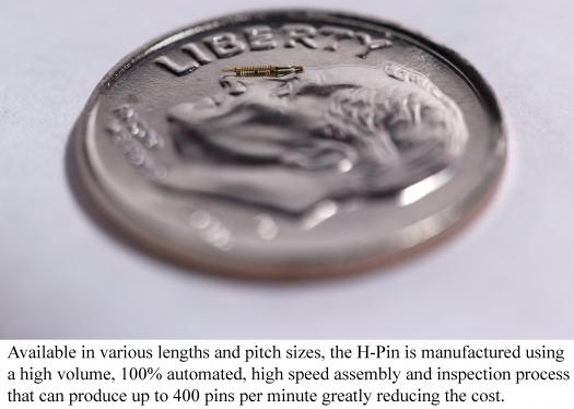
Although there are a few design tweaks, the real departure is in the manner in which complete pin assemblies are manufactured using a high volume BeCu stamping process and a 100% automated, high speed assembly and inspection process that can produce up to 400 pins per minute.
Available in various lengths and pitch sizes as low as .2mm, the product is the brainchild of Plastronics, a global provider of test sockets for semiconductor reliability testing. For more than 40 years, the company has used spring-loaded probe pins to create finished sockets for burn-in, humidity, failure analysis and other test requirements.
Depending on quantities, the spring-loaded probe pins can cost 30-50 percent less. With thousands of pins potentially in a single test socket or board-to-board connector, the savings can be significant.
According to Taylor, simply reducing the cost meant little without consistent pin quality. To ensure this was the case, EP Ants conducted extensive testing of the H-pin, which included inviting customers to also test the product and provide additional feedback.
"As a test socket manufacturer, we have to rely on the quality of the pins we get from our spring probe supplier," says Taylor. "The H-pins have a very reliable quality level which is extremely important to us and our customers."
Meeting High Performance Demands
For spring-loaded probes pins, high performance characteristics are defined by the ability to withstand high temperatures required for burn-in and other tests, ability to handle increasing amounts of current over increasingly smaller pins, and the ability to handle high frequencies.
According to Taylor, they do not rely on a single pin manufacturer. However, his company uses the H-pins for high temperature burn-in, tri-temp and HAST testing where the spring-probe is regularly subjected to temperatures well in excess of 200°C.
"The H-Pin works well when exposed to the high temperatures we use for burn-in or tri-temp testing," says Taylor. The tests are typically conducted at up to 240°C and, despite cooling the back side, the spring pins still experiences a fair amount of temperature. "We have worked with these pins above 200 degrees and we did not have a problem where other pins have failed."
The ability of the pins to withstand higher levels of current, despite shrinking in size, is also an increasing concern "“ particularly with the prevalence of higher power output lithium batteries.
"These semiconductor packages and chips have power management features that need to be tested as well," says Taylor. "The H-pins can take a lot of current."
For high performance applications, there can be concerns about the construction of traditional spring-loaded probe pins and how its design can affect the quality of the connection under compression, the potential for unreliable test results requires all finished pins be tested and binned according to performance results. A very costly process step.
According to Ironwood Electronics' Ila Pal, the H-Pin solves this problem by utilizing a leaf spring between the two plungers along with external compression spring that allows the pin to maintain a good connection and pass signal throughout its movement.
Furthermore, the performance of the pin as measured by its contact resistance is also a benefit in high frequency testing. Whereas standard spring-loaded probe pins can experience wide variations in contact resistance, potentially leading to false failures, the variation in the H-Pin is minimal and well within accepted levels.
"For the H-Pins, the variation is very minimal," says Pal. "So, testing is very precise, because we can add a cut-off factor for pass and fail, without having to worry about false failures."
David Pfaff - President

Mr. Pfaff is President of Plastronics Socket Company. He has run Plastronics Socket Company, a fully integrated design, injection mold and manufacturer of burn-in sockets, for over 10 years. Mr. Pfaff graduated from Pomona College and has a MBA from the University of Texas at Austin. He has served on the board of the Entrepreneurs Organization in Dallas for the past 7 years. He lives in Irving, Texas, with his wife and two beautiful children.


