
Smallest diamonds used to make electrical wires three atoms wide
Researchers have devised a way to use the smallest possible bits of diamond to put various types of atoms together Lego-style into the thinnest possible electrical wires just three atoms wide.
The new technique, reported in Nature Materials, could potentially be used to build tiny wires for a wide range of applications, including fabrics that generate electricity, optoelectronic devices that employ both electricity and light, and superconducting materials that conduct electricity without any loss.
The diamondoids used by researchers at Stanford University and Stanford Linear Accelerator Center (SLAC) National Accelerator Laboratory, a U.S. Department of Energy facility, as assembly tools are tiny, interlocking cages of carbon and hydrogen. Found naturally in petroleum fluids, they are extracted and separated by size and geometry in a SLAC laboratory.
Over the past decade, a research program at Stanford Institute for Materials and Energy Sciences (SIMES) led by Nicholas Melosh, co-author of the new study and an associate professor at SLAC and Stanford, and SLAC/Stanford Professor Zhi-Xun Shen has found a number of potential uses for the little diamonds, including improving electron microscope images and making tiny electronic gadgets.
While there are other ways to get materials to self-assemble, the new method allows researchers to assemble those materials with atom-by-atom precision and control, and this is the first one shown to make a nanowire with a solid, crystalline core that has good electronic properties, said Melosh, adding that the minuscule size is important, because a material that exists in just one or two dimensions - as atomic-scale dots, wires or sheets - can have very different, extraordinary properties compared to the same material made in bulk.
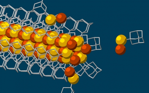
The researchers started with the diamondoids, namely single cages that contain just 10 carbon atoms, and attached a sulfur atom to each. Floating in a solution, each sulfur atom bonded with a single copper ion, creating the basic nanowire building block. The building blocks then drifted toward each other, drawn by the van der Waals attraction between the diamondoids, and attached to the growing tip of the nanowire. The result is needle-like wires with a semiconducting core, which is a combination of copper and sulfur known as a chalcogenide, surrounded by the attached diamondoids, which form an insulating shell.
"Much like Lego blocks, they only fit together in certain ways that are determined by their size and shape," Stanford graduate student Fei Hua Li, who played a critical role in synthesizing the tiny wires and figuring out how they grew, was quoted as explaining in a news release from Stanford. "The copper and sulfur atoms of each building block wound up in the middle, forming the conductive core of the wire, and the bulkier diamondoids wound up on the outside, forming the insulating shell."
The team has used diamondoids to make one-dimensional nanowires based on cadmium, zinc, iron and silver, including some that grew long enough to see without a microscope, and experimented with carrying out the reactions in different solvents and with other types of rigid, cage-like molecules, such as carboranes. The cadmium-based wires are similar to materials used in optoelectronics, such as light-emitting diodes (LEDs), and the zinc-based ones are like those used in solar applications and in piezoelectric energy generators, which convert motion into electricity.
"This method gives us a versatile toolkit where we can tinker with a number of ingredients and experimental conditions to create new materials with finely tuned electronic properties and interesting physics," Melosh noted.
"What we have shown here is that we can make tiny, conductive wires of the smallest possible size that essentially assemble themselves," said Hao Yan, a Stanford postdoctoral researcher and lead author of the paper. "The process is a simple, one-pot synthesis. You dump the ingredients together and you can get results in half an hour. It's almost as if the diamondoids know where they want to go."


