
Intel $7 Billion Investment in Next-Gen Semiconductor Factory
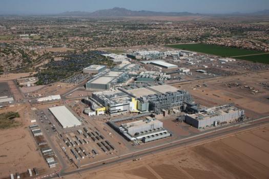
Intel Corporation has announced plans to invest more than $7 billion to complete Fab 42, which is expected to be the most advanced semiconductor factory in the world. The high-volume factory is in Chandler, Ariz., and is targeted to use the 7 nanometre (nm) manufacturing process. It will produce microprocessors to power data centres and hundreds of millions of smart and connected devices worldwide. The announcement was made by U.S. President Donald Trump and Intel CEO Brian Krzanich at the White House.
The completion of Fab 42 in 3 to 4 years will directly create approximately 3,000 high-tech, high-wage Intel jobs for process engineers, equipment technicians, and facilities-support engineers and technicians who will work at the site. Combined with the indirect impact on businesses that will help support the factory's operations, Fab 42 is expected to create more than 10,000 total long-term jobs in Arizona.
"Intel's business continues to grow and investment in manufacturing capacity and R&D ensures that the pace of Moore's law continues to march on, fueling technology innovations the world loves and depends on," said Krzanich. "This factory will help the U.S. maintain its position as the global leader in the semiconductor industry."
"Intel is a global manufacturing and technology company, yet we think of ourselves as a leading American innovation enterprise," Krzanich added. "America has a unique combination of talent, a vibrant business environment and access to global markets, which has enabled U.S. companies like Intel to foster economic growth and innovation. Our factories support jobs "” high-wage, high-tech manufacturing jobs that are the economic engines of the states where they are located."
Intel is America's largest high-technology capital expenditure investor ($5.1 billion in the U.S. 2015) and its third largest investor in global R&D ($12.1 billion in 20151). The majority of Intel's manufacturing and R&D is in the United States. As a result, Intel employs more than 50,000 people in the United States, while directly supporting almost half a million other U.S. jobs across a range of industries, including semiconductor tooling, software, logistics, channels, OEMs and other manufacturers that incorporate our products into theirs.
The 7 nm semiconductor manufacturing process targeted for Fab 42 will be the most advanced semiconductor process technology used in the world and represents the future of Moore's Law. In 1968 Intel co-founder Gordon Moore predicted that computing power will become significantly more capable and yet cost less year after year.
Making a leading-edge computer chip is the most complex manufacturing process in the world, engineering magic that turns sand into semiconductors, the foundation of the knowledge economy.
The chips made on the 7 nm process will power the most sophisticated computers, data centres, sensors and other high-tech devices, and enable things like artificial intelligence, more advanced cars and transportation services, breakthroughs in medical research and treatment, and more. These are areas that depend upon having the highest amount of computing power, access to the fastest networks, the most data storage, the smallest chip sizes, and other benefits that come from advancing Moore's Law.


