
UnitySC Receives Multiple Orders For Wafer Thinning Inspection Systems
UnitySC, a supplier of advanced inspection and metrology solutions, has announced multiple orders from a leading integrated device manufacturer (IDM) for its modular 4See Series automated defect inspection platform. The systems were selected because they deliver optimal wafer backside surface and edge defect inspection, post thinning and metallization. The 4See Series will be used for automotive applications by a market leader in power semiconductor manufacturing to improve the reliability and performance of its products.
"Being selected by a market leader validates the strength of our solutions and confirms our strategy to address new markets with our advanced process control solutions," said Gilles Fresquet, CEO, UnitySC. "This win expands our reach beyond the traditional substrate control market to include wafer thinning for power semiconductors."
IHS Markit predicts USD $3 billion in global market growth for the power semiconductors used in cars and light passenger vehicles, over the next six years. Increasing electronic content is a key driver, particularly in hybrid and electric cars, due to consumer demand for constant connectivity. The automotive industry's push to deliver autonomous, green vehicles in the next decade is also driving growth. These technologies rely on the latest power semiconductor devices, enabled by advanced wafer manufacturing processes like wafer thinning.
"As the wafers used in power semiconductor manufacturing become thinner, controlling wafer quality through the backside thinning and metallization process steps becomes more critical to end-device performance and reliability," noted Fresquet. "For years, manufacturers have considered our Deflector module to be the best-in-class solution for silicon and silicon-on-insulator wafer slip line detection. Combined with the Edge module, this 4See Series configuration delivers industry-leading inspection capabilities that meet semiconductor market needs."
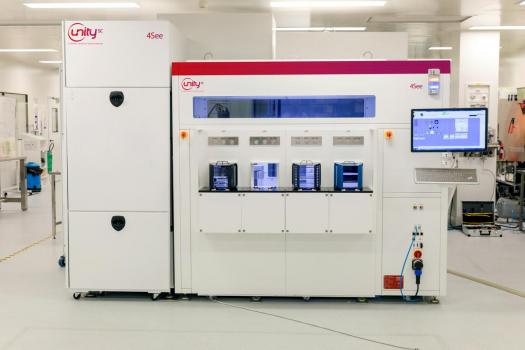
UnitySC's new 4See Series for all-surface inspection of semiconductor wafers is a modular system with up to three module offerings: Deflector, Edge and LineScan. The platform can be configured according to application needs, such as wafer thinning, µbumping, MEMS, and more, and can include any number of the modules in desired configurations.
"¢ Based on phase shift deflectometry technology, the Deflector module is a wafer surface inspection solution that achieves high throughput and very high vertical sensitivity in the nanometer range. It can detect slip lines, grinding marks, failures, cracks, comets, embedded particles, residue, and stains. The Deflector module is well suited to frontside and backside inspection, even under highly warped conditions.
"¢ The Edge module is a high throughput and versatile solution based on confocal chromatic technology, which is used to inspect the full wafer edge: top, top bevel, apex, bottom bevel and bottom. It has a high depth of focus and does not require a backside contact chuck.
Combining the Deflector and Edge modules in one system offers full wafer characterization compliant with 8" or 12'' wafer high-volume manufacturing requirements. The 4See Series is scheduled to ship in Q3 2017 to fab locations around the world.


