
Rudolph Lithography System Advances Panel-based Advanced Packaging
Rudolph Technologies has announced that it has received an order for its JetStep S Lithography System for fan-out panel level processing. The system, which will ship in June 2017 to an outsourced assembly and test (OSAT) facility based in Asia, will be used to produce system-in-package (SiP) products that combine sensor, processor and memory functions for the automotive industry.
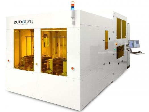
"Inherently large in size with a rectangular form factor, a SiP is ideally suited for panel manufacturing," said Rich Rogoff, vice president and general manager of Rudolph's Lithography Systems Group. "Panels can accommodate a higher number of SiPs, which reduces the cost of manufacturing advanced packages due to the rectangular shape and large surface area. Generally speaking, a typical panel would allow approximately 150 percent more devices to be processed compared to wafer-level processes. The JetStep S System was selected because of its ability to process very large panel sizes up to 650mm x 720mm and its large field size that optimizes throughput for larger packages."
Rogoff continued, "We see an increasing number of manufacturers investing in panel processing technology across a variety of applications, including SiP and large die processing for multiple high-end technologies. This is an exciting transition for our customers and we are pleased that the JetStep system's unique combination of imaging and handling capabilities is helping early adopters more quickly prove out the cost of ownership benefits of panel processing."
Moving from round wafers to rectangular panels saves corner space, delivering a roughly ten-percent improvement in surface utilization. The larger size of the substrate and the improved fit between the mask and substrate maximizes the number of packages on a given substrate, which reduces the transfer overhead by a factor of five. Beyond advanced packaging lithography, Rudolph also offers process control solutions for panel manufacturing, including defect inspection and closed loop analytics software to drive tighter process capability and ramp to yield.


