
Stripping costs out of photo resist processing
Redesigned
wet processing tool significantly extends photoresist stripping bath life,
providing dramatic savings on chemicals and disposal costs says
Ryan Zrno chief technical officer of JST Manufacturing
Silicon and compound semiconductor wafers undergo many critical procedures during the microfabrication process, including the recurring stripping of photoresist, the light-sensitive material (liquid or film) that is deposited during various steps of wafer production. Re-examining the wet process of stripping of thick photoresist, which occurs at the back-end of wafer processing, can significantly reduce the amount of chemicals required, as well as related disposal costs.
Photoresist materials are designed to mask, or "resist," the UV light to accomplish back-end-of-line tasks such as the etching and electroplating of circuits and copper pillars used as bonding pads for wafer packaging. In recent years, wafer foundries as well as semiconductor and compound semiconductor manufacturers have begun to incorporate copper pillars into their fabrication processes. The advantages of copper over solder have become increasingly important, including the use of higher pin counts and interconnect densities; copper also offers higher reliability and improved electrical and thermal performance.
It is noteworthy that back-end processes require the use of solvents while front-end-of-line processes, typically employ acids such as sulfuric acid and peroxide. These would attack surfaces such as copper pillars in a destructive manner. Also, back-end processes use much thicker photoresist materials and because the solvents used for back-end stripping are less aggressive, chunks of un-dissolved resist residue often accumulate in the bath. These chunks can block bath circulation and filtration, shortening bath life and increasing solvent chemistry consumption substantially.

Evaluating wet processing challenges After recently deciding to adopt copper pillars for the wafers it produces in-house, a wafer manufacturer unexpectedly ran into some production obstacles. Two situations caused the manufacturer to rethink the process by which it stripped the "thick" resist from its wafers during the copper pillar attachment process. Both situations were connected directly to the chemical bath tool that was integral to the stripping process.
"Our customer, an amplifier manufacturer, was dealing with a 50-100 micron thick resist film on its wafers, about 15 times thicker than resist used on front-end processes," explains Ryan Zrno chief technical officer of JST Manufacturing, a specialist in wet processing equipment for the MEMS, nano, photovoltaic, wafer and related industries. "Using the traditional solvent chemistry was leaving large amounts of chunky resist residue in the bath, which was interfering with both circulation and filtration. This was causing increased bath changes resulting in production delays and excessive use of expensive chemical solvents.
" Zrno adds that the customer also wanted to find an alternative to the TMAH (Tetramethylammonium hydroxide) -based solvent that had been used in the past. Although not used in toxic amounts, this solvent had an offensive odor and was not the most effective chemical for resist stripping around wafer with copper pillars.
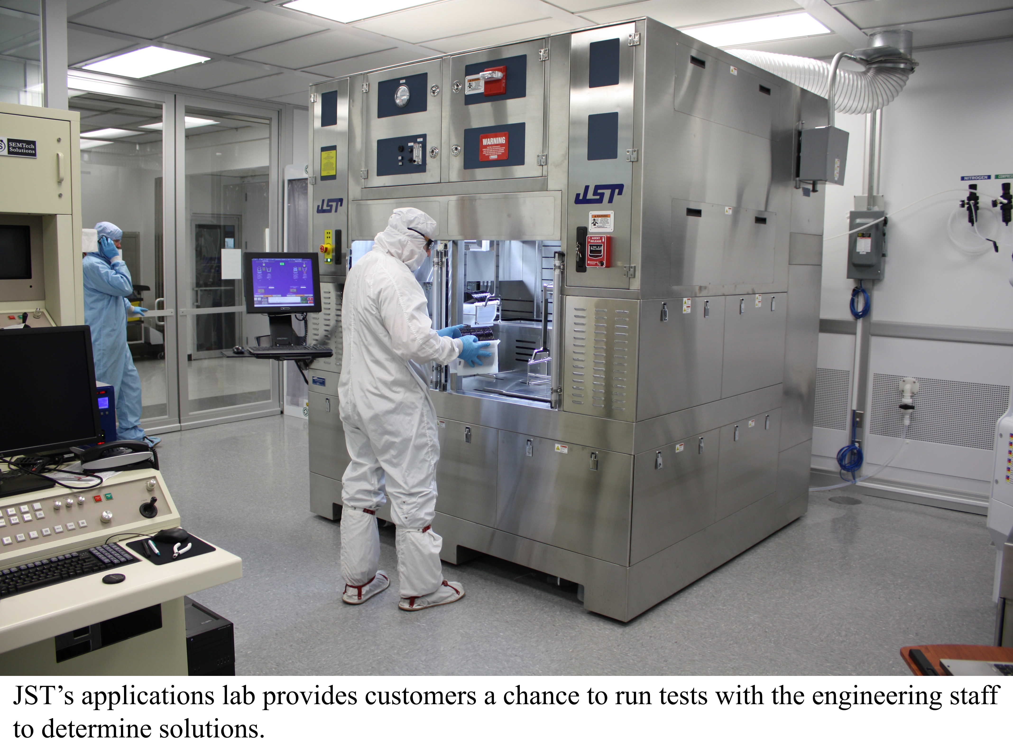
To evaluate the problems and propose optimum solutions, Zrno invited the customer to visit JST's applications lab and run some tests with the engineering staff. The company also coordinated a series of tests with appropriate solvents made to order from Diamalloy, the customer's chemical supplier. Building an optimum solution "We ran a set of three different kinds of tests, each in our standard down flow bath tool," Zrno says.
"Each time we would learn something valuable about possible solutions. It was a three-way development team composed of the customer's staff, the chemical company, and our engineers." After a few weeks of testing the proposed solution was a new wet processing tool that did not leave large deposits of solubilized resist in the bath. Instead, a new chemistry was recommended along with a series of screens that were incorporated into quick-dump exchanges. This meant that the bath solvent chemistry was circulated in such a manner that it flowed over the screens, removing any large clusters of resist before they could become totally solubilized and prematurely deplete the effectiveness of the bath solvent. Removal of resist clusters also meant that they were no longer a threat to bath filtration or circulation. The next step was we built a test module, which included a bath with a single series of screens, a reservoir, basic control system, and a pump.
"Once completed the customer came back out and we did testing again," Zrno says. "After successful testing of the module, JST designed and built a fully-automated production tool featuring a 6-gallon bath and 20-gallon reservoir. We also added other proprietary components that enabled the tool to meet the customer's production requirements."
The customer ordered two of the new production tools in order to run parallel processes and meet throughput requirements. A combination of savings As anticipated, this new, automated resist-stripping tool saved on chemical usage, and the series of screens prevented the recirculating bath chemistry from plugging up the filters.
Chemical usage dropped by two-thirds at the customer's resists stripping stations, mainly due to the increased bath life. Also significant were the savings on downtime requirements for changing of baths, which normally took 30 to 60 minutes. Those were also reduced by two-thirds, as was the associated downtime to drain and recharge bath solutions. The cost of disposing of the spent chemistry is also considerable, although it varies according to location.
For example, a leading waste management company advertises pickup and disposal of toxic chemical substances for $1.49 per pound for complete service. A 55-gallon barrel of water-based liquid weight approximately 460 lbs. Based on $1.49 per pound, the cost of having a waste specialist dispose of that liquid would cost roughly $685. Reducing that cost by two-thirds via a system like the wet processing tool described above would amount to a savings of $456 per barrel.
Other savings can be achieved as well. For example, the new resist stripping station includes a menu of built-in settings, which were tested and installed at the JST factory lab. This menu makes it unnecessary for users to go to another facility to establish new settings, a process that could increase production downtime by up to several days.
According to Zrno, it usually makes a lot of sense to periodically review your production systems such as wet processing equipment, particularly when production procedures change. In many cases making minor modifications to existing equipment, whether standard or custom, can save companies significant money over time.


