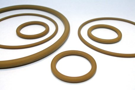
PPE launch new plasma resistant elastomer materials

Precision Polymer Engineering has announced the launch of two new elastomer materials which dramatically improve durability and increase sealing performance in a variety of applications within the semiconductor industry.
The two new perfluoroelastomers (FFKM) have been formulated to deliver low plasma erosion rates and increased seal lifetime with minimal particle generation. Following comprehensive testing using different plasma chemistries and plasma sources, the results show the new materials perform better than their closest competitors, with a 30% reduction in erosion rates in some cases. Both materials boast low trace metal content, which reduces the risk of lower yield and warranty failures.
Commenting on the launch of the new materials, Dr Murat Gulcur, Product Manager for Semiconductor at PPE, said: "Aggressive plasma chemistries have always been a major challenge for our customers, and with the extensive testing and subsequent launch of Perlast G65HP and Perlast G67G, we believe we can give our customers market-leading performance against all other elastomer sealing technologies under the same conditions "“ along with significant cost savings.".
PPE developed the new high purity materials to meet the needs of critical applications where seals are in direct contact with the process chemistry or in close proximity to the wafer. They are expected to provide extended lifetime that is compatible with existing maintenance cycles, potentially increasing the process tool uptime, leading to an overall lower cost of consumables.
A closer look at the PPE's new Perlast materials Perlast G65HP is made up of a unique organic formulation, specifically designed to minimise the risk of particle generation. This material is ideal for critical semiconductor applications at advanced technology nodes, it maintains the integrity of device electrical specifications and minimises reliability failures. Perlast G65HP provides excellent resistance to very aggressive radical rich fluorine plasmas, resulting in extended maintenance cycles and lower cost of consumables.
Perlast G67G offers much improved resistance to aggressive oxygen, chlorine and fluorine-based plasmas. With low levels of nano-particle fillers, the risk contamination is much less likely. The plasma resistance of this material is maximised by dispersing individual nano-particle fillers uniformly throughout the polymer matrix. This material provides outstanding thermal and mechanical properties and low particle generation, Perlast® G67G is ideally suited to dry etching, stripping, cleaning and PVD processes


