
Taming "Wild" Electrons in Graphene
Discovery could lead to novel electronic devices
Graphene "“ a one-atom-thick layer of the stuff in pencils "“ is a better conductor than copper and is very promising for electronic devices, but with one catch: Electrons that move through it can't be stopped. Until now, that is. Scientists at Rutgers University-New Brunswick have learned how to tame the unruly electrons in graphene, paving the way for the ultra-fast transport of electrons with low loss of energy in novel systems. Their study was published online in Nature Nanotechnology.
"This shows we can electrically control the electrons in graphene," said Eva Y. Andrei, Board of Governors professor in Rutgers' Department of Physics and Astronomy in the School of Arts and Sciences and the study's senior author. "In the past, we couldn't do it. This is the reason people thought that one could not make devices like transistors that require switching with graphene, because their electrons run wild."
Now it may become possible to realize a graphene nano-scale transistor, Andrei said. Thus far, graphene electronics components include ultrafast amplifiers, supercapacitors and ultralow resistivity wires. The addition of a graphene transistor would be an important step towards an all-graphene electronics platform. Other graphene-based applications include ultrasensitive chemical and biological sensors, filters for desalination and water purification. Graphene is also being developed in flat flexible screens, and paintable and printable electronic circuits. Graphene is a nano-thin layer of the carbon-based graphite that pencils write with. It is far stronger than steel and a great conductor. But when electrons move through it, they do so in straight lines and their high velocity does not change.
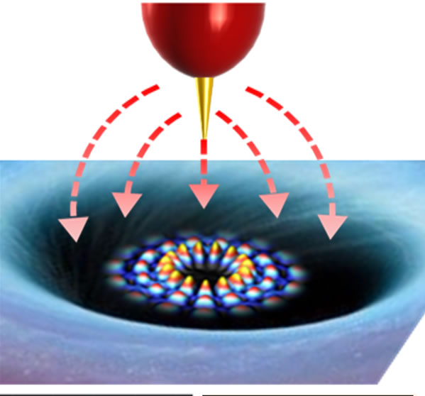
"If they hit a barrier, they can't turn back, so they have to go through it," Andrei said. "People have been looking at how to control or tame these electrons." Her team managed to tame these wild electrons by sending voltage through a high-tech microscope with an extremely sharp tip, also the size of one atom. They created what resembles an optical system by sending voltage through a scanning tunneling microscope, which offers 3-D views of surfaces at the atomic scale. The microscope's sharp tip creates a force field that traps electrons in graphene or modifies their trajectories, similar to the effect a lens has on light rays. Electrons can easily be trapped and released, providing an efficient on-off switching mechanism, according to Andrei.
"You can trap electrons without making holes in the graphene," she said. "If you change the voltage, you can release the electrons. So you can catch them and let them go at will."
The next step would be to scale up by putting extremely thin wires, called nanowires, on top of graphene and controlling the electrons with voltages, she said. The study's co-lead authors are Yuhang Jiang and Jinhai Mao, Rutgers postdoctoral fellows, and a graduate student at Universiteit Antwerpen in Belgium. The other Rutgers co-author is Guohong Li, a research associate.


