
Ultra-Thin Memory Storage Device Paves Way for Powerful Computing
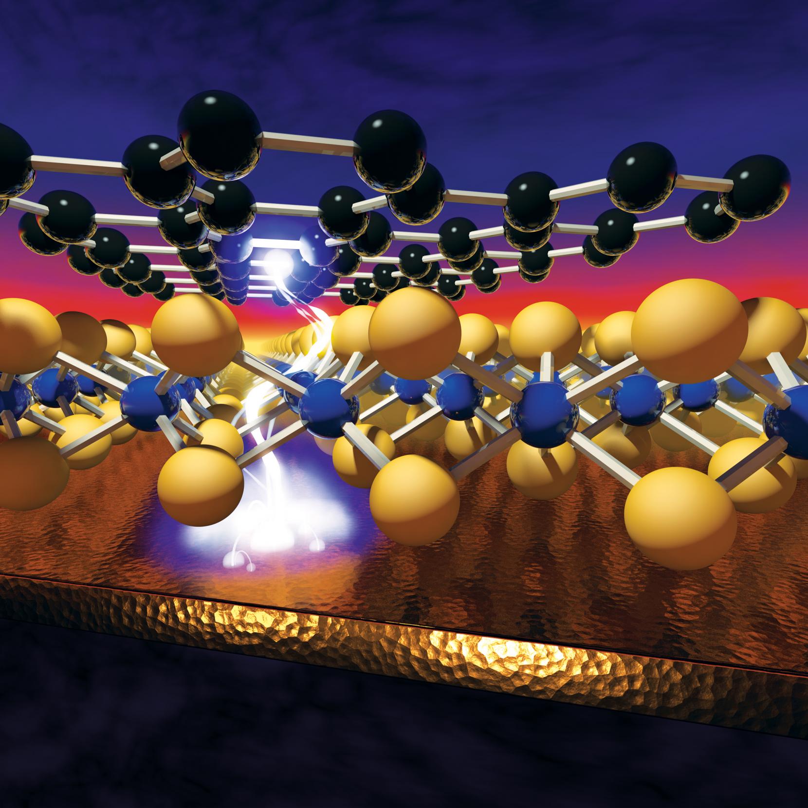
Illustration of a voltage-induced memory effect in monolayer nanomaterials, which layer to create "atomristors," the thinnest memory storage device that could lead to faster, smaller and smarter computer chips. Cockrell School of Engineering
Engineers worldwide have been developing alternative ways to provide greater memory storage capacity on even smaller computer chips. Previous research into two-dimensional atomic sheets for memory storage has failed to uncover their potential "” until now.
A team of electrical engineers at The University of Texas at Austin, in collaboration with Peking University scientists, has developed the thinnest memory storage device with dense memory capacity, paving the way for faster, smaller and smarter computer chips for everything from consumer electronics to big data to brain-inspired computing.
"For a long time, the consensus was that it wasn't possible to make memory devices from materials that were only one atomic layer thick," said Deji Akinwande, associate professor in the Cockrell School of Engineering's Department of Electrical and Computer Engineering. "With our new "˜atomristors,' we have shown it is indeed possible."
Made from 2-D nanomaterials, the "atomristors" "” a term Akinwande coined "” improve upon memristors, an emerging memory storage technology with lower memory scalability. He and his team published their findings in the January issue of Nano Letters.
"Atomristors will allow for the advancement of Moore's Law at the system level by enabling the 3-D integration of nanoscale memory with nanoscale transistors on the same chip for advanced computing systems," Akinwande said.
Memory storage and transistors have, to date, always been separate components on a microchip, but atomristors combine both functions on a single, more efficient computer system. By using metallic atomic sheets (graphene) as electrodes and semiconducting atomic sheets (molybdenum sulfide) as the active layer, the entire memory cell is a sandwich about 1.5 nanometers thick, which makes it possible to densely pack atomristors layer by layer in a plane. This is a substantial advantage over conventional flash memory, which occupies far larger space. In addition, the thinness allows for faster and more efficient electric current flow.
Given their size, capacity and integration flexibility, atomristors can be packed together to make advanced 3-D chips that are crucial to the successful development of brain-inspired computing. One of the greatest challenges in this burgeoning field of engineering is how to make a memory architecture with 3-D connections akin to those found in the human brain.
"The sheer density of memory storage that can be made possible by layering these synthetic atomic sheets onto each other, coupled with integrated transistor design, means we can potentially make computers that learn and remember the same way our brains do," Akinwande said.
The research team also discovered another unique application for the technology. In existing ubiquitous devices such as smartphones and tablets, radio frequency switches are used to connect incoming signals from the antenna to one of the many wireless communication bands in order for different parts of a device to communicate and cooperate with one another. This activity can significantly affect a smartphone's battery life.
The atomristors are the smallest radio frequency memory switches to be demonstrated with no DC battery consumption, which can ultimately lead to longer battery life.
"Overall, we feel that this discovery has real commercialization value as it won't disrupt existing technologies," Akinwande said. "Rather, it has been designed to complement and integrate with the silicon chips already in use in modern tech devices."
Funding for the UT Austin team's work was provided by the National Science Foundation and the Presidential Early Career Award for Scientists and Engineers, which Akinwande was awarded in 2015.


