
LETI proposes curving technology for optical equipment
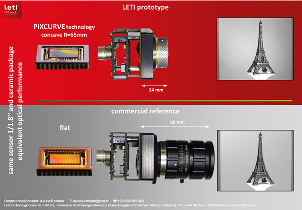
Fig. 1: Leti's prototype with PIXCURVE technology compared to a commercial reference: performance improves, while size, complexity and cost are reduced.
Leti, a research institute at CEA Tech, has developed a new curving technology for optical sensors and micro-displays that improves performance, enhances field of view and compensates for aberrations in optical applications.
The technology curves components such as CMOS imagers and charged-couple device (CCD) imagers for mobile phones, cameras, telescopes, medical-imaging tools and industrial-control equipment. Other uses include IR sensors for astronomy, defense, drones and micro-displays for automotive applications, augmented reality and virtual reality.
Leti's fully functional prototype of this technology was presented today in the paper, "Curved Sensors for Compact High-Resolution Wide Field Designs: Prototype Demonstration and Optical Characterization", at Photonics West 2018, in collaboration with LAM (Laboratoire d'Astrophysique de Marseille). Called PIXCURVE, it also is being demonstrated at Leti's booth, 431, in the Moscone Center, where the conference is based.
"Curved sensor technology is a disruptive approach for imaging applications such as photography, videography, computer vision, surveillance and many other applications," said Bertrand Chambion, one of the paper's co-authors. "In recent years, we have seen very strong interest in curved electronics, particularly for opto-electronics systems whose performance improves, while size, complexity and cost are reduced."
The demonstration is based on a 1/1.8'' format, 1.3-million-pixel CMOS image sensor. The standard sensor structure consists of a 7.74 x 8.12 mm silicon die glued on a ceramic package. Electrical connections are wire bonded from the die to the package surface and, then, to the interconnection board. A glass cover is placed on top for mechanical protection.
Leti's technology uses a grinding process to get the sensor below 100µm thick, which makes it mechanically flexible. It is then glued onto a curved substrate, which determines its final shape. A wire bonding process developed for electrical connections is used to prevent damages on the thinned dies. The radius of curvature is R=65mm. This prototype is compared to the equivalent commercial solution with flat sensor in Figure 1.
This process is compatible with any sensor size and with large-scale manufacturing processes


