
New sensor for measuring electric field strength
TU Wien has developed a sensor for measuring the strength of electric fields, which is smaller, simpler and less prone to distortion than comparable devices.
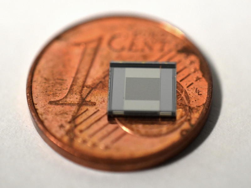
Picture: Tiny new sensor - compared to a one-cent-coin
Accurately measuring electric fields is important in a variety of applications, such as weather forecasting, process control on industrial machinery, or ensuring the safety of people working on high-voltage power lines. Yet from a technological perspective, this is no easy task.
In a break from the design principle that has been followed by all other measuring devices to date, a research team at TU Wien has now developed a silicon-based sensor as a microelectromechanical system (MEMS). Devised in conjunction with the Department for Integrated Sensor Systems at Danube University Krems, this sensor has the major advantage that it does not distort the very electric field it is currently measuring. An introduction to the new sensor has also been published in the electronics journal "Nature Electronics".

A moveable grid made of silicon is displaced in an electric field, relative to another grid, which is fixed.
"The equipment currently used to measure electric field strength has some significant downsides," explains Andreas Kainz from the Institute of Sensor and Actuator Systems (Faculty of Electrical Engineering, TU Wien). "These devices contain parts that become electrically charged. Conductive metallic components can significantly alter the field being measured; an effect that becomes even more pronounced if the device also has to be grounded to provide a reference point for the measurement." Such equipment also tends to be relatively impractical and difficult to transport.
The sensor developed by the team at TU Wien is made from silicon and is based on a very simple concept: small, grid-shaped silicon structures measuring just a few micrometres in size are fixed onto a small spring. When the silicon is exposed to an electric field, a force is exerted on the silicon crystals, causing the spring to slightly compress or extend.
These tiny movements now need to be made visible, for which an optical solution has been designed: an additional grid located above the movable silicon grid is lined up so precisely that the grid openings on one grid are concealed by the other. When an electric field is present, the movable structure moves slightly out of perfect alignment with the fixed grid, allowing light to pass through the openings. This light is measured, from which the strength of the electric field can be calculated by an appropriately calibrated device.
Prototype achieves impressive levels of precision
The new silicon sensor does not measure the direction of the electric field, but its strength. It can be used for fields of a relatively low frequency of up to one kilohertz. "Using our prototype, we have been able to reliably measure weak fields of less than 200 volts per metre," says Andreas Kainz. "This means our system is already performing at roughly the same level as existing products, even though it is significantly smaller and much simpler." And there is still a great deal of potential for improvement, too: "Other methods of measurement are already mature approaches "“ we are just starting out. In future it will certainly be possible to achieve even significantly better results with our microelectromechanical sensor," adds Andreas Kainz confidently.

Schematics of the sensor: the moveable and the fixed grid


