
Brewer Science Introduces Cost-Effective Alternative for Advanced-Node Wafer Patterning
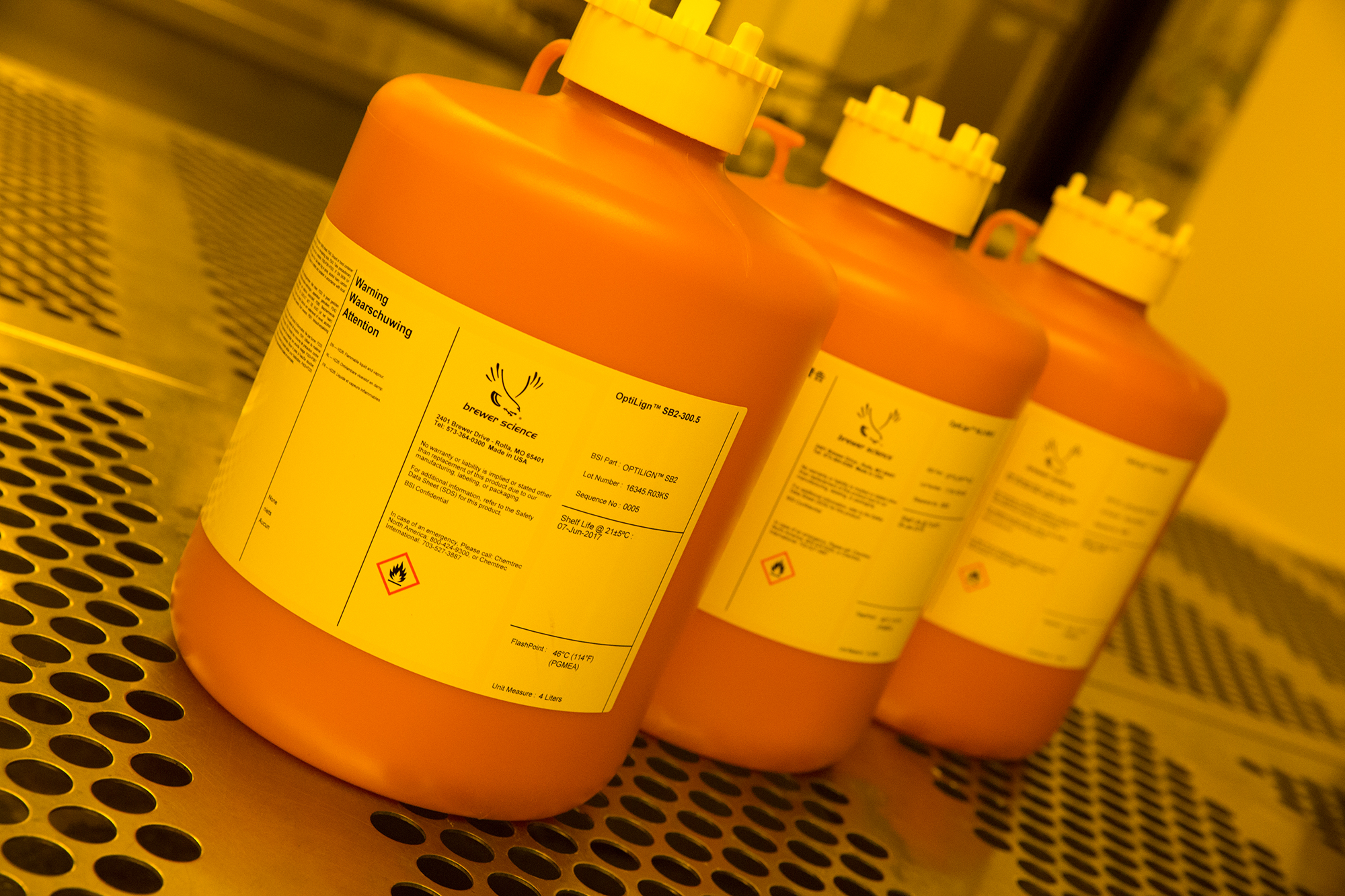
Brewer Science, from the SPIE Advanced Lithography 2018 conference, has introduced its OptiLign™ commercial-quality directed self-assembly (DSA) material set developed in collaboration with Arkema. The OptiLign system currently includes three materials required for self-assembly: block copolymers, neutral layers and guiding layers. Developed together for optimal performance, these DSA materials are manufactured on Brewer Science's commercial manufacturing equipment and provide a cost-effective path to advanced-node wafer patterning processes for feature sizes down to 12 nm.
Although Moore's law is slowing, many foundries and integrated device manufacturers are continuing efforts to scale to finer nodes. As feature sizes shrink more aggressively with each node, the limits of manufacturing equipment are being stretched, and it has become cost-prohibitive to create them using existing patterning processes like self-aligned double patterning and self-aligned quadruple patterning. While the industry is close to the commercialization of extreme ultraviolet (EUV) lithography, the tool cost will limit its use. DSA offers an alternative to existing processes and can be performed on existing, installed fab tool sets. Additionally, DSA will serve as a complement to EUV when it becomes fully available.
"Taking OptiLign materials from pilot line to commercial-scale production represents the next significant milestone in making DSA a viable option for semiconductor manufacturing," said Dr. Srikanth (Sri) Kommu, executive director, Semiconductor Business, Brewer Science Inc. "Historically, the industry has relied on equipment enhancements to reach the next technology node. Now, materials solutions are stepping in to provide that edge and extend tool capabilities. The OptiLign product family is an example of this paradigm shift."
Brewer Science's OptiLign family of DSA products provides all the materials needed for self-assembly, according to the company. Block copolymers define the pattern. Neutral layers allow the pattern to be formed on each layer. Lastly, guiding layers tell the material which way and how to orient. All the materials are designed to work together for optimal performance, and are dependent on material and surface energy. Additionally, through its partnership with Arkema, Brewer Science has tapped into a way to deliver DSA materials that allows for consistent feature sizes via a unique polymer production process. This process allows for the large scale needed to support an entire technology node, as well as a unique polymer quality and reproducibility, all of which sets OptiLign materials apart from the competition.
"Feature size is built into the molecular structure of the DSA materials and can vary from batch to batch, so securing a sub-nanometric reproducibility can be challenging," explained Dr. Ian Cayrefourcq, Director of Emerging Technologies, Arkema. "Arkema's special process for formulating large batches of polymers of the same size allows Brewer Science to supply a fab with consistent feature sizes for the technology node's life span


