
Memory Sector Poised for MRAM Shakeup
Silicon Valley newcomer Spin Transfer Technologies believes their approach to magnetoresistive random access memory (MRAM) may reset computer memory paradigms through dramatically improved retention paired with sizably smaller current consumption.
Memory technologies including SRAM (static random-access memory) and dynamic random-access memory (DRAM) dominate global computing and data processing markets. But each approach to storing critical data has density and other performance limits that have led to a slowing of traditional semiconductor scaling in memory sectors. Manufacturers have sought alternatives that would support traditional memory usages as well as emerging markets including the IoT, autonomous vehicles, artificial intelligence and burgeoning sensor and photonics markets.
MRAM has emerged as a clear leader amongst competing memory technologies hoping to unseat SRAM and DRAM dominance. But like most integrated semiconductor technologies there are frequently performance tradeoffs and compromises that affect serviceability and cost. Research has continued to increase the competitiveness of MRAM while retaining its unique advantages including non-volatility and the fact that it utilizes magnetic energy to manipulate the spin of electrons to control a bit's resistance, thus allowing programmers to create the 1s and 0s that form the basis of all digital memory systems, yet without some of the electron-based limits of SRAM and DRAM technology.
A key participant in the race pursuing MRAM enhancements is Spin Transfer Technologies (Fremont, California) which announced the results of a stealth development program on 30th April that the company believes offers memory developers and manufacturers significant advantages compared to existing MRAM processes. Along with improved performance, STT indicated in its announcement that the technology adds negligible costs to existing CMOS processes and can be accomplished with existing equipment already owned by the world's leading semiconductor fabricators.
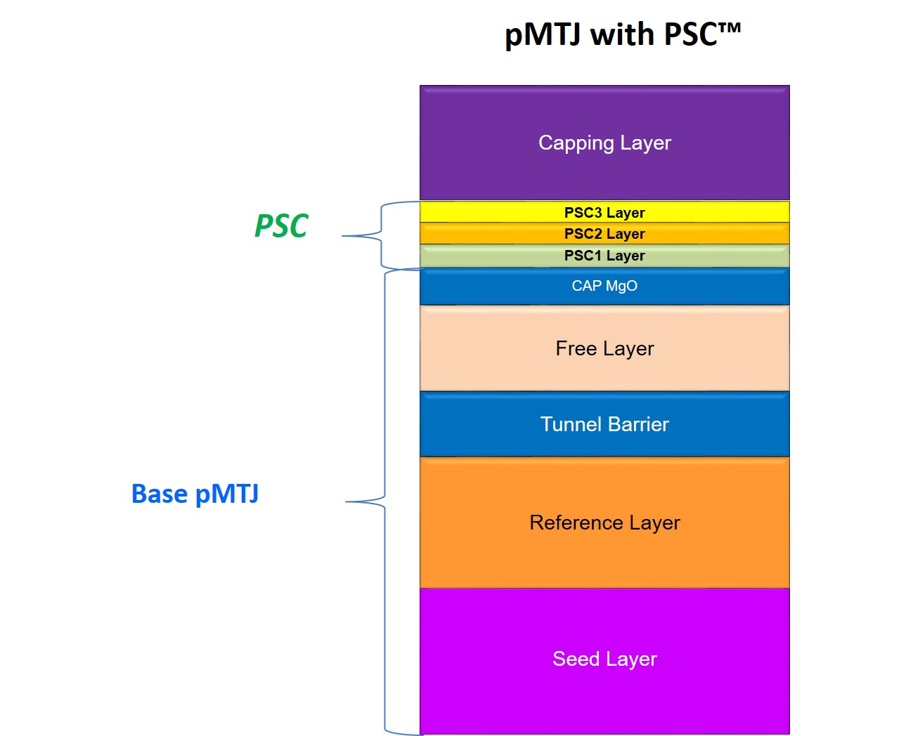
STT, in an announcement at the Intermag applied magnetism conference held recently in Singapore, described their new proprietary technique as Precessional Spin Current (PSC™), a modular approach to performance enhancements that can be applicable to any company's MRAM designs. While there are a number of approaches to creating an MRAM including magnetic field switching, STT's approach is designed to enhance the performance and retention of spin polarized current that is utilized to affect a memory bit's state.
STT said their PSC technology will increase the spin-torque efficiency of any MRAM device between 40 and 70 percent. According to the company, this technique enables any MRAM to achieve dramatically higher data retention while consuming less power. This gain translates into dramatically increased retention times as great as 10,000 times longer than MRAM's without PSC (e.g., 1 hour retention becomes more than 1 year retention) "“ all while reducing current consumption. Data that STT collected also shows that PSC structural efficiency gains actually increase as perpendicular magnetic tunnel junctions (pMTJs) get smaller. The company said it believes these factors mean their PSC structure could lead to achieving embedded SRAMs in the latest 7 nm and 5 nm device generations. The PSC structure is a breakthrough because it effectively decouples the static energy barrier that determines retention from the dynamic switching processes that govern the switching current, they noted.
Before making their public announcement, STT invited industry analysts who are expert in memory device evolution, development and manufacturing to examine the company's performance data and comment on the potential of Precessional Spin Current technology to enhance MRAM performance.
"Emerging applications, especially those using batteries, such as AR/VR, IoT and many machine learning applications need non-volatile alternatives to SRAM and DRAM," said Tom Coughlin, president of Coughlin Associates, Inc. "STT MRAM will enable these technologies to do more with less power."
Also invited to review STT's latest innovation was Jim Handy, general director of Objective Analysis. Silicon Semiconductor spoke to Handy, asking about factors that have held back MRAM to date and prospects for PSC MRAM in future electronic end-use devices.
"MRAM is attracting a lot of attention as an embedded memory for ASICs and MCUs, but issues of write current and data retention have caused concern," said Handy. "Spin Transfer Technologies' new PSC structure shows a lot of promise to solve a number of those issues and pave the path for MRAM to take a significant share of the embedded memory market."
Commenting further, Handy noted, "MRAM has widespread appeal. In mobile applications, particularly in the Internet of Things, MRAM may provide a path to reduce energy consumption to lengthen battery life when it is used as the on-chip memory in an ASIC or MCU. The data center is likely to see some use of MRAM in SoCs that might be used as processors or controllers. It will be a number of years, though, before MRAM is used to replace DRAM and NAND flash. You ask where it's most applicable. Objective Analysis and Coughlin Associates are working on a report, to be published in late May, which covers emerging memory technologies. We find that MRAM and other technologies will find their first success in embedded memories (memories in ASICs, MCUs, etc.) that are built using standard CMOS logic processes on advanced process nodes (45nm and finer pitches)."
Spin Transfer Technologies' testing of the PSC structure involved comparing the performance of the same pMTJ devices with and without PSC for a large number of memory chips within CMOS test arrays at various temperatures and device diameters. STT said the tests exhibited a robust performance advantage due to the PSC structure, both during writing of the low-resistance ("0") and the high-resistance ("1") memory states. Specific advantages include the following samples:
· Increase of the spin-torque efficiency by up to 70 percent
· Demonstration of the efficiency gain across a range of sizes (40-60 nm) and temperatures (30°C to 125°C)
· Increase of the thermal energy barriers by 50 percent corresponding to an increase in data retention time of greater than four orders of magnitude while reducing the switching current
· Reduction of read disturb error rate up to five orders of magnitude
"There is a huge demand for a memory with the endurance of SRAM, but with higher density, lower operating power and with non-volatility. We believe the improvements the PSC structure brings to STT-MRAM technology will make it a highly attractive alternative to SRAM for these reasons," said Mustafa Pinarbasi, CTO and SVP of Magnetics Technology at Spin Transfer Technologies. "We are excited to enable the next generation of STT-MRAM and to shake up the status quo of the memory industry through our innovation."
The company indicated that it is in discussion with multiple manufacturers regarding interest in the Precessional Spin Current technology and STT's continuing development activities.
Re Image: Spin Transfer Technologies said its new Precessional Spin Current (PSC) structure can increase the efficiency of MRAM devices 40-70% while adding no more than 4 nm to a device's height.


