+44 (0)24 7671 8970
More publications     •     Advertise with us     •     Contact us
 
News Article

Orbotech and IME to develop advanced packaging solutions

News

Orbotech a global supplier of yield-enhancing and process-enabling solutions for the manufacture of electronics products, and A*STAR's Institute of Microelectronics (IME), have announced a joint lab agreement confirming Orbotech as a partner in IME's FOWLP joint lab and as a member of the IME FOWLP development line consortium.

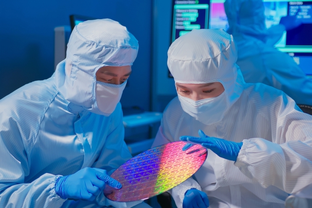
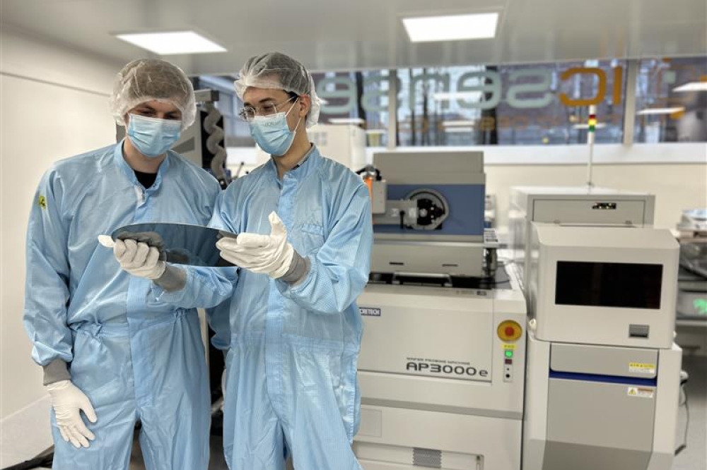
Orbotech's Emerald UV Laser Drilling solution is one of the key processes available in the FOWLP joint lab development line. The Emerald delivers advanced UV drilling performance for today's most challenging IC substrate and assembly applications, including 3D packages, stacking and package on package.

The FOWLP development line at IME's facilities at Singapore Science Park II, and its new facilities at Fusionopolis Two, will allow IME and its partners to develop technologies that will serve a wide range of markets including consumer electronics, healthcare and automotive.

"Orbotech is honored to be part of IME's FOWLP development joint lab and FOWLP development line consortium," said Dr. Abraham Gross, Corporate Executive Vice President, Chief Technology Officer and Head of Innovation of Orbotech. "This collaboration builds on the long-term relationship that IME has with Orbotech's SPTS Technologies, a leading supplier of advanced packaging solutions. We are always pleased to cooperate with technology and process innovation initiatives that push the electronics packaging industry forward and enable solutions for complex challenges. The Emerald UV Laser Drilling system is just one of the building blocks that we, at Orbotech, provide to enhance the quality and efficiency of the production process for 3D IC and other complex high density packaging structures."

Purdue, imec, Indiana announce partnership
Resilinc partners with SEMI on supply chain resilience
NIO and NXP collaborate on 4D imaging radar deployment
Panasonic Industry digitally transforms with Blue Yonder
Global semiconductor sales decrease 8.7%
MIT engineers “grow” atomically thin transistors on top of computer chips
Keysight joins TSMC Open Innovation Platform 3DFabric Alliance
Leti Innovation Days to explore microelectronics’ transformational role
Quantum expansion
indie launches 'breakthrough' 120 GHz radar transceiver
Wafer fab equipment - facing uncertain times?
Renesas expands focus on India
Neuralink selects Takano Wafer Particle Measurement System
Micron reveals committee members
Avoiding unscheduled downtime in with Preventive Vacuum Service
NFC chip market size to surpass US$ 7.6 billion
Fujifilm breaks ground on new €30 million European expansion
Fraunhofer IIS/EAS selects Achronix embedded FPGAs
Siemens announces certifications for TSMC’s latest processes
EU Chips Act triggers further €7.4bn investment
ASE recognised for excellence by Texas Instruments
Atomera signs license agreement with STMicroelectronics
Gartner forecasts worldwide semiconductor revenue to decline 11% in 2023
CHIPS for America outlines vision for the National Semiconductor Technology Center
TSMC showcases new technology developments
Alphawave Semi showcases 3nm connectivity solutions
Greene Tweed to open new facility in Korea
Infineon enables next-generation automotive E/E architectures
Global AFM market to reach $861.5 million
Cepton expands proprietary chipset
Semtech adds two industry veterans to board of directors
Specialty gas expansion
×
Search the news archive

To close this popup you can press escape or click the close icon.
Logo
×
Logo
×
Register - Step 1

You may choose to subscribe to the Silicon Semiconductor Magazine, the Silicon Semiconductor Newsletter, or both. You may also request additional information if required, before submitting your application.


Please subscribe me to:


You chose the industry type of "Other"

Please enter the industry that you work in: