Perovskite-on-silicon: a nanometric sandwich

Research teams at Ecole Polytechnique Federale de Lausanne (EPFL) and the CSEM PV-centre in Switzerland have integrated a perovskite cell directly on top of a standard silicon-based cell, obtaining a record efficiency of 25.2 percent. The research has been published in Nature Materials.
Their production method is promising, they say, because it would add only a few extra steps to the current silicon-cell production process, and the cost would be reasonable.
Perovskite's unique properties have prompted a great deal of research into its use in solar cells over the last few years. In the space of nine years, the efficiency of these cells has risen by a factor of six. Perovskite allows high conversion efficiency to be achieved at a potentially limited production cost.
In tandem cells, perovskite complements silicon: it converts blue and green light more efficiently, while silicon is better at converting red and infra-red light. "By combining the two materials, we can maximises the use of the solar spectrum and increase the amount of power generated. The calculations and work we have done show that a 30 percent efficiency should soon be possible," say the study's main authors Florent Sahli and Jérémie Werner.
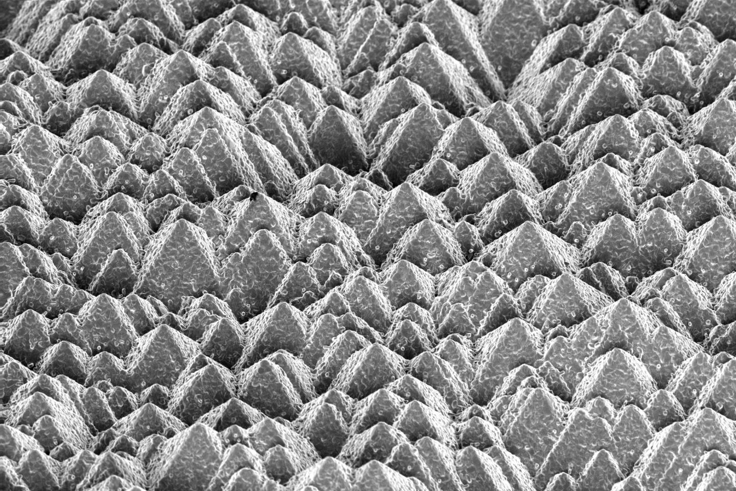
However, creating an effective tandem structure by superposing the two materials is no easy task. "Silicon's surface consists of a series of pyramids measuring around 5 microns, which trap light and prevent it from being reflected. However, the surface texture makes it hard to deposit a homogeneous film of perovskite," explains Quentin Jeangros, who co-authored the paper.
When the perovskite is deposited in liquid form, as it usually is, it accumulates in the valleys between the pyramids while leaving the peaks uncovered, leading to short circuits.
Scientists at EPFL and CSEM have worked around that problem by using evaporation methods to form an inorganic base layer that fully covers the pyramids. That layer is porous, enabling it to retain the liquid organic solution that is then added using a thin-film deposition technique called spin-coating. The researchers subsequently heat the substrate to a relatively low temperature of 150degC to crystallize a homogeneous film of perovskite on top of the silicon pyramids.
"Until now, the standard approach for making a perovskite/silicon tandem cell was to level off the pyramids of the silicon cell, which decreased its optical properties and therefore its performance, before depositing the perovskite cell on top of it. It also added steps to the manufacturing process," says Florent Sahli.
Updating existing technologies
The new type of tandem cell is highly efficient and directly compatible with monocrystalline silicon-based technologies, which benefit from long-standing industrial expertise and are already being produced profitably. "We are proposing to use equipment that is already in use, just adding a few specific stages. Manufacturers won't be adopting a whole new solar technology, but simply updating the production lines they are already using for silicon-based cells," explains Christophe Ballif, head of EPFL's Photovoltaics Laboratory and CSEM's PV-Center.
At the moment, research is continuing in order to increase efficiency further and give the perovskite film more long-term stability. Although the team has made a breakthrough, there is still work to be done before their technology can be adopted commercially.
'Fully textured monolithic perovskite/silicon tandem solar cells with 25.2% power conversion efficiency' by F. Sahli et al; Nature Materials, 2018


